Geoscience Reference
In-Depth Information
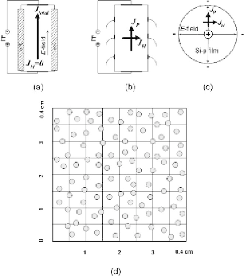
Fig. 10.5.
Geometry of the applied electric
E
and magnetic
B
0
fields, as well as the
Pedersen current
J
P
(alongtheelectricfield),Hallcurrent
J
H
(across
E
and
B
0
)
and a total current
J
T
. The magnetic field oriented inside the page. a) Open Hall
circuit. Non-conductive walls prevent the
J
H
flow. The vertical thin arrow represents
the applied electrical field, while the bold arrow represents the total current as a
consequence of the combined Pedersen current produced by the initial electric field
as well as of the Hall current due to the polarized electric field between the walls.
A potential difference was applied to the side surfaces of the rectangular plate. b)
Closed Hall circuit in which
J
H
can leak independently of
J
P
. c) The measurements
on the closed Hall circuit were taken on a thin (0.05 cm) disk-shaped plate with an
aperture at the center. An electric field between large and small radii of the disk
excites a circular ring of Hall current enclosed and circulating around the axis of the
disk. d) Enlarged fragment of the mask (0.4
×
0.4 cm). Different areas of the mask
had different transparency
Free carriers were generated by an illumination passing through a filter of
pure Si and a mask pressed to the sample. The mask was a thin sapphire plate
200 µm thick. On a mask sized 4
×
4 mm there were 100 transparent spots sized
2
L
p
∼
440 µm
(see Fig. 10.5). The detailed description of the experiment may be found in
[7]. The variability of inhomogeneities, that is, the ratio of transparency in a
spot to transparency outside the spot (in the negative mask) was 0
.
8.
The magnetic field was in the range 0
<B<
30kGs ( 0
<β
e
<
15).
200 µm. The mean distance between the spot centers was 2
L
c
∼
Search WWH ::

Custom Search