Environmental Engineering Reference
In-Depth Information
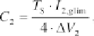
(4.78)
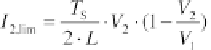
This is obtained from the mean input current and the reciprocal of the duty
cycle. If the mean output current
I
2
is lower than:
(4.79)
the current through the inductance during the switch blocking phase decreases
until it reaches zero. The diode will then block the current and the voltage at
the inductance becomes zero. The voltage and current thus go into a
discontinuous operation mode. A suitable sizing of components can avoid this.
If the limiting lower current
I
2,lim
is known, the inductance can then be sized
by:
(4.80)
Switching frequencies
f
=1/
T
between 20 kHz and 200 kHz seems to be a
good compromise. The output capacity
C
2
is obtained by:
(4.81)
using the ripple of the output voltage
V
2
, i.e. the maximum desired voltage
fluctuation
V
2
.
Semiconductor components such as power field-effect bipolar transistors,
or thyristors, for higher powers are mainly used for the switch S. Some
integrated circuits (IC) exist that can directly control the duty period. For small
power applications, the transistors are already integrated into some ICs.
∆
Boost converters
Boost converters are suitable for applications with higher output voltages than
input voltages. The principle boost converter structure is similar to that of the
buck converter, except that the diode, switch and inductance change positions.
Figure 4.37 shows the boost converter circuit.
If the switch
S
is closed, a magnetic field is created in the inductance
L
with the voltage
v
L
=
V
1
(
v
L
> 0). When the switch opens, the voltage
v
2
=
V
1
-
v
L
(
v
L
< 0) is applied to the load. This voltage is higher than the input
voltage
V
1
. In this case, the voltage drop at the diode has been neglected. When
the switch closes, the capacitor
C
2
retains the load voltage. The diode
D
avoids
the discharging of the capacitor through the switch
S
.