Hardware Reference
In-Depth Information
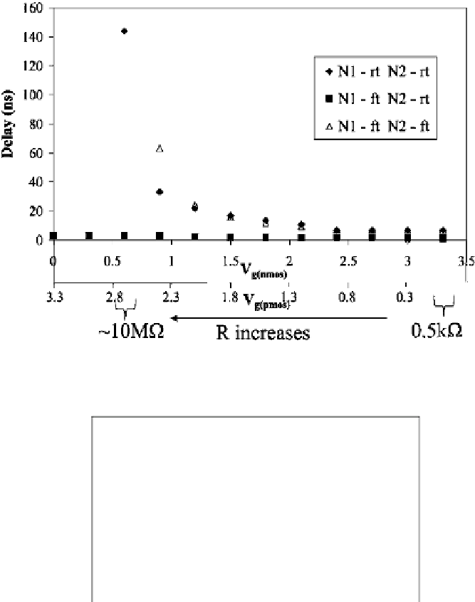
Fig. 1.12
Experimental delay results for
resistive
opens with neighbors changing their state, rt:
rising transition, ft: falling transition
(
Arumı et al.
2008a
)
6.5
Slow corner
Experimental
6
Nom
i
na
l
5.5
5
F
a
st
co
r
ne
r
4.5
0.0
0.2
0.4
0.6
0.8
1.0
Open location (
a
)
Fig. 1.13
Experimental and simulation delay results for low
resistive
open defects (
Arumı
of the transistor network driving the defective line, the parasitic capacitances and
the threshold voltage of the transistors driven by the defective net. Experimental
evidence of this is presented by
Arum´ıetal.
(
2008c
)
. Figure
1.13
summarizes ex-
perimental and simulation results obtained with low
resistive
opens (a few k). The
delay is higher when the open is located in the middle of the interconnect line related
to the rest of locations, i.e., the beginning and the end of the line.