Hardware Reference
In-Depth Information
The MCP2551 can be placed in the standby or sleep mode by applying a high voltage at the
R
S
pin. In sleep mode, the transmitter is switched off, and the receiver operates at a lower cur-
rent. The receive pin on the controller side (RxD) is still functioning but will operate at a slower
rate. The attached microcontroller can monitor the RxD pin for CAN bus activity and place the
transceiver into normal operation via the R
S
pin.
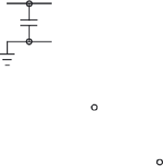
A typical method of interfacing the MCP2551 transceiver to the HCS12 CAN module is
shown in Figure 13.45. The maximum achievable bus length in a CAN bus network is deter-
mined by the following physical factors:
1. The loop delay of the connected bus nodes (CAN controller and transceiver) and the
delay of the bus line.
2. The differences in bit time quantum length due to the relative oscillator tolerance
between nodes.
3. The signal amplitude drop due to the series resistance of the bus cable and the input
resistance of bus node.
The resultant equation after taking these three factors into account would be very com-
plicated. The bus length that can be achieved as a function of the bit rate in the high-speed
mode and with CAN bit timing parameters being optimized for maximum propagation delay is
HCS12
TXCAN
RXCAN
TxD
RxD
V
REF
R
S
R
EXT
5 V
V
CC
100 nF
MCP2551
GND
CANH
CANL
R
EXT
set to 0 in high-
speed mode
CAN_H
CAN bus line
120
Ω
120
Ω
CAN_L
Figure 13.45
■
Interfacing the MCP2551 with the HCS12


Search WWH ::

Custom Search