Biomedical Engineering Reference
In-Depth Information
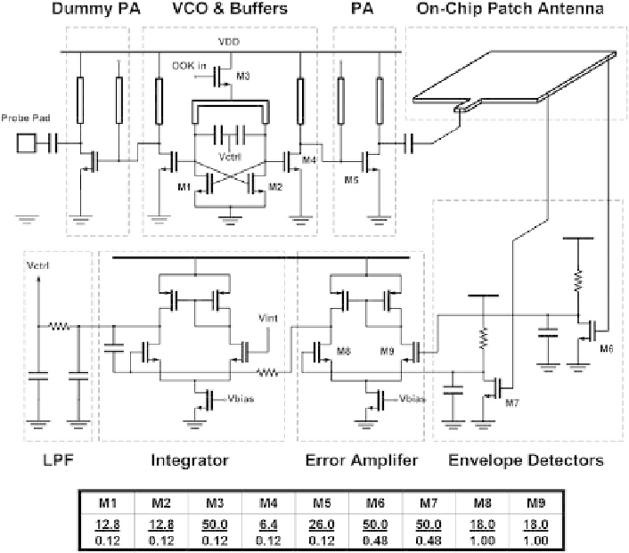
Fig. 16
Schematic of the 60-GHz frequency-locked loop (FLL).
VCO
voltage-controlled oscillator,
PA
power amplifier,
LPF
low-pass filter
regulated by the feedback baseband part. The VCO is designed to be on-off keying
(OOK) modulated by power gating with a PMOS header device, so that the FLL can
serve as a simple low-rate OOK transmitter. Note that the baseband circuits high-
lighted in Fig.
15
are placed beneath the patch antenna ground plane using Metal 1
to Metal 3 routing layers.
Figure
16
shows the schematic of the 60-GHz FLL. The VCO uses a cross-coupled
pair topology with an LC resonator. The resonator is realized by a half-wavelength
transmission line at the top metal layer, and the simulated Q-factor of the resonator
is 15 at 60 GHz. The frequency tuning is achieved by a pair of thin oxide negative-
channel metal-oxide semiconductor (NMOS) varactors. One of the differential VCO
outputs feeds the signal onto the patch antenna through a common source stage buffer
and a PA. The PA is designed for maximum power delivery, using the top metal layer
for high-Q transmission lines for matching. Ideally, we want to probe the signal at
the antenna input, where the FLL output is. However, the pad and probing might
destroy the matching condition between the PA and the antenna, so the secondary
output of the differential VCO is used for testing and is connected to an RF probe
Search WWH ::

Custom Search