Graphics Reference
In-Depth Information
Twisting reduces Precharge
and Activate commands
64x64 pixel block
01
45
0
0x00
0x01
0x02
0x03
0x04
0x05
0x06
0x07
01
0x08
0x09
0x0A
0x0B
0x0C 0x0D 0x0E
0x0F
0x10
0x11
0x12
0x13
0x14
0x15
0x16
0x17
23
67
45
0
Col Addr: 0x17
7b00101
11
67
23
256x128 pixel block
Same row address
in each bank
0
8x4 pixel MAU Tiling
7bit Column Address
Last 2bits: Cache Datapath
23
0x78
0x79
0x7A
0x7B
0x7C 0x7D 0x7E
0x7F
DRAM Latency Aware
Memory Mapping
0
1 2
3
0
1
Cache Datapath Index
2
3
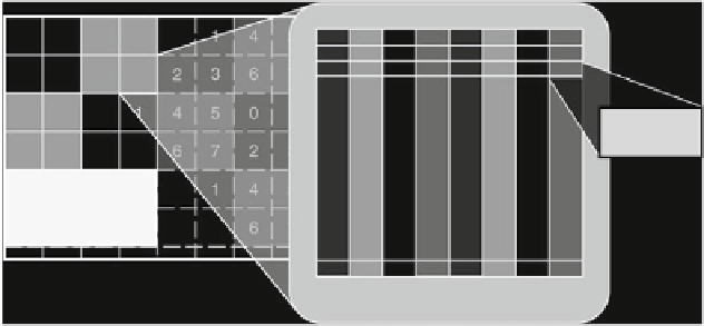
Fig. 10.14
4 MAUs arranged in raster scan order make
up one block. The twisted structure increases the horizontal distance between two rows in the same
bank. Note how the MAU columns are partitioned into four datapaths (based on the last 2 bits of
column address) for the four-parallel cache architecture
Latency Aware DRAM mapping. 128 8
10.6.1
DRAM Latency Aware Memory Map
An ideal mapping of pixels to DRAM addresses should minimize the number of
DRAM accesses and the latency experienced by each access. This can be achieved
by minimizing the fetch of unused pixels and the number of row precharge/activate
operations respectively. Note that the above optimization only fixes how the pixels
are stored in DRAM and can be performed even in the absence of an MC cache.
Also, the DRAM addresses should be mapped to cache lines such that conflict
misses are minimized. To enable a coherent presentation, we explain these ideas
with respect to a specific memory map. The underlying principles are quite general
and can be easily reused.
Figure
10.14
shows an example latency aware memory map. The luma color
plane of a picture is tiled by 256
128 pixel blocks in raster scan order. Each block
maps to an entire row across all eight banks. These blocks are then broken into
eight 64
64 blocks which map to an individual bank in each row. Within each
64
64 block, 32-byte MAUs map to 8
4 pixel blocks that are tiled in a raster scan
order. In Fig.
10.14
, the numbered square blocks correspond to 64
64 pixels and
the numbers stand for the bank they belong to. Note how the mapping of 128
128
pixel blocks within each 256
128 regions alternates from left to right. Figure
10.14
shows this twisting behavior for a 128
128 pixel region composed of four 64
64
blocks that map to banks 0, 1, 2 and 3.
The chroma color plane is stored in a similar manner in different rows. The
only notable difference is that an 8
4 chroma MAU is composed of pixel-level
interleaving of 4
4 U and V blocks. This is done to exploit the fact that U and V
have the same reference region.