Biomedical Engineering Reference
In-Depth Information
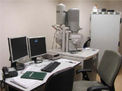
figure 6.7
Nova NanoSEM 230 scanning electron microscope from fEI Company.
mag
1000 x
HV
2.00 kV
spot
4.5
det
ETD
WD
5.1 mm
HFW
298 µm
100 µm
NRF-NNIN at WUStL
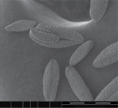
figure 6.8
Scanning electron micrograph of plant pollen on carbon tape sputter coated
with gold before imaging.
a conductive material such as gold. In cases where sputter coating is not desirable,
charging effects on nonconductive sample may be reduced by using lower acceler-
ating voltages or by using the low-vacuum or environmental mode available on some
SEMs (fig. 6.10). In low-vacuum mode, charging effects on nonconductive samples
are eliminated by introducing water or solvent vapor into the sample chamber at the
expense of some resolution and contrast.
Search WWH ::

Custom Search