Environmental Engineering Reference
In-Depth Information
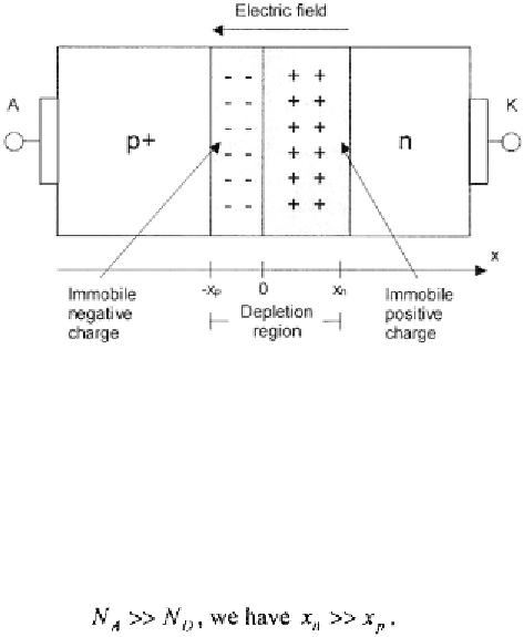
meaning that this side is
doped more heavily (in the order of than its n-type
counterpart (in the order of that is This is not
a limitation since most pn junctions are built with one side more heavily
doped than the other.
Close to the junction, free electrons on the n side are attracted by free
positive charges on the p side so they diffuse across the junction and
recombine with holes. Similarly, holes on the p side are attracted by
electrons on the n side, diffuse across the junction and recombine with free
electrons on the n side.
Note that the p-type section is denoted with
This phenomenon leaves behind positive ions (or immobile positive
charges) on the n side, and negative ions (or immobile negative charges) on
the p side, thus creating a depletion region across the junction where no free
carriers exist. Moreover, since charge neutrality obliges the total amount of
charge on one side to be equal to the total amount of charge on the other, the
width of the depletion region is greater on the more lightly doped side, that
is, in our case where
Due to immobile charges, an electric field appears from the n side to the p
side and generates the so-called built-in potential of the junction. This
potential prevents further net movement of free charges across the junction
under open circuit and steady-state conditions. It is given by [1]-[2]