Image Processing Reference
In-Depth Information
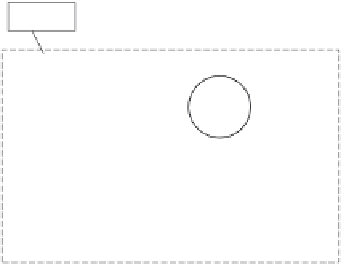
Pixel
V
dd
RST
Reset
pulse
Drive
transistor
Reset
transistor
V
out
Source follower amplifier
C
in
Q
sig
PD
Voltage gain:
G
V
Vertical
signal line
RS
Row select
transistor
Row select
pulse
∆
V
out
= (
Q
sig
/
C
in
)
G
V
Q
out
C
sl
Load transistor gate bias
Load
transistor
V
ss
FIGURE 5.39
Three-transistor pixel configuration.
be seen as the FDA forming with drive and load transistors discussed in Sections 2.3.1 and
2.3.2 by regarding
C
in
as
C
dif
. Generated charges
Q
sig
are integrated in the
n
-region of the
PD, whose potential is initially reset to
VV
in
=
( )
, and resulting potential
V
i
sig
is expressed
by the following equation, where
Q
sig
includes polarity of signal charge, that is,
Q
sig
should
be negative in the case of electrons:
0
dd
VV
Q
C
sig
(5.3)
*
sig
0
=+
in
in
in
Thus, the potential of the
n
-region changes from
V
i
0
to
V
i
sig
by generated signal charges.
Expressing voltage gain of the SFA as
G
V; the gate threshold voltage of the drive transistor
as
Vt
h; amount of voltage change of
n
-region (input amplitude) as
Δ
Vi
n; and SFA outputs
as
V
out
at inputs
V
i
0
and
V
i
sig
, respectively, the amount of voltage change of output
(output amplitude) and stored signal charge quantity
Q
out
at output capacitance
C
sl
are
shown as follows:
sig
0
and
V
out
(
)
0
0
=−
(5.4)
VVVG
V
out
in
th
Q
C
VG
(
)
sig
sig
sig
0
(5.5)
VVVG V
=
−
=+−
out
in
th
V
in
th
V
in
Q
C
sig
sig
0
∆
VVV
=−=
(5.6)
in
in
in
in
*
Since this expression includes polarity of charge, it is [+
Q
sig
]. If the signal charge is electrons, then [
Q
sig
] should
be negative.