Environmental Engineering Reference
In-Depth Information
(a)
(b)
5
10
0 nm
60 nm
120 nm
180 nm
active layer
8
0
6
-5
cathode
an
o
de
4
0 nm
60 nm
120 nm
180 nm
2
-10
0
-0.3
0.0
0.3
0.6
0.9
0
30
60
90
120
150
180
Bias (V)
Position in the active layer (nm)
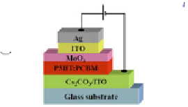
Fig. 8 a Electrical characteristics, recorded under AM 1.5G illumination (100 mW cm
-2
), of
inverted OPVs incorporating ITO optical spacers of various thicknesses; inset: device
architecture of an OPV incorporating an ITO optical spacer. b Calculated distribution profiles
of the exciton generation rate within the active layer for OPV devices incorporating optical
spacers of various thicknesses; inset: schematic representation of the layer stack [
41
]
Unfortunately, the work function of ITO (ca. 4.7 eV) was somehow misaligned
with the HOMO energy levels of the polymers, imposing an energy barrier for hole
collection at the electrodes. Therefore, we incorporated a layer of MoO
3
, which
has a high work function (ca. 5.3 eV), to decrease the contact resistance. The
reference device exhibited a value of V
oc
of 0.59 V, a value of J
sc
of
9.54 mA cm
-2
, and a FF of 0.67, yielding a PCE of 3.76 %. The value of V
oc
of
the device remained at 0.59 V after incorporating the optical spacer. By tuning the
thickness of the ITO layer, the value of J
sc
increased to 11.49 mA cm
-2
. Although
the FF decreased slightly to 0.62, presumably due to the increased resistance
arising from the presence of ITO and/or possible sputtering damage, its effect was
overwhelmed by the much higher photocurrent. Overall, the PCE improved to
4.20 %. To understand the mechanism responsible for the enhanced device per-
formance, we calculated the ideal exciton generation rate within the active layer
(Fig.
8
b). After integrating the area beneath the curves, we found that the optical
spacers failed to increase the total number of excitons, presumably due to the
film's sufficient thickness, which had been optimized. When the ITO thickness was
120 nm, however, we could still successfully shift the exciton generation zone
away from the electrodes and diminish any possible quenching process at the
electrodes, thereby increasing the photocurrent in real devices.
4.2 Surface Plasmonic Effects
Surface plasmons are confined electromagnetic waves propagating along the sur-
face of a conductor [
43
-
55
]; they have many unique properties, including local field
enhancement and strong light scattering, which might improve the absorption
process in OPVs. Plasmonic structures for enhancing OPV performance can be


Search WWH ::

Custom Search