Environmental Engineering Reference
In-Depth Information
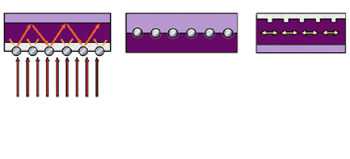
(a)
(b)
(c)
Fig. 9 Plasmonic structures for increasing the efficiency of OPVs. a Metal NPs at the thin film
surface can scatter most incident light into the material having the higher dielectric constant,
helping to confine the photons in the device. b Metal NPs embedded in the semiconductor
materials; the induced SPs can enhance the near-field in the structure. c A periodic structure at the
back metal electrode induces SPPs; this structure can turn the incident photons by 90 [
44
]
generally divided into three categories (Fig.
9
)[
44
]. In the first case, metal nano-
particles (NPs; e.g., Cu, Ag, Pt, or Au NPs), which can trigger localized surface
plasmon resonance (LSPR), are placed in front of the active thin film in the OPV
(Fig.
9
a). In contrast to light scattering in a homogeneous medium, light will be
scattered preferentially into the material having the larger permittivity. Subse-
quently, through multiple and/or high-angle scattering, the overall optical path
length increases, thereby improving the absorption efficiency of the OPV. Figure
9
b
displays the second possible structure, in which the NPs are embedded directly into
the organic semiconducting layer [
44
]. Because the absorption is proportional to the
intensity of the electromagnetic field, the enhanced near-field induced by the SPs
can increase the absorption efficiency [
45
]. In the third case, surface plasmon
polaritons (SPPs) propagating at the metal-semiconductor interface are excited by
metal nanostructures (e.g., periodic arrays or gratings) (Fig.
9
c) and the induced
evanescent electromagnetic fields are confined near the interface. Therefore, light is
turned by 90 in such a structure. Because photons are absorbed along the lateral
direction, the optical length of which is several orders of magnitude longer than the
thickness of the semiconductor layer, the absorption efficiency can be increased
significantly.
Many remarkable plasmonic approaches have been proposed to increase the
light absorption efficiency of OPVs. For example, in 2008, Kim et al. fabricated
Ag NPs through pulse-current (PC) electrodeposition onto ITO substrates
(Fig.
10
a) [
46
]. This electrochemical approach was used to control the size,
density, and morphology of the NP films. The authors fabricated relatively uniform
Ag NPs having an average particle size of approximately 13 nm (inset to
Fig.
10
a). As a result, the device PCE improved from 3.05 to 3.69 % after
incorporation of these Ag NPs. They attributed the increased photocurrent to the
SPR effect induced by the metal NPs. Similarly, Morfa et al. deposited Ag NPs
through conventional thermal evaporation on ITO-coated glass substrates; a layer
of PEDOT:PSS was subsequently deposited onto the NPs [
47
]. Figure
10
b dis-
plays the device structure. The PCE of the device increased from 1.3 ± 0.2 to


Search WWH ::

Custom Search