Environmental Engineering Reference
In-Depth Information
Table 8.2 Photovoltaic parameters of the PSCs with NPs incorporated in different layers under
AM 1.5G illumination at 100 mW/cm
2
. R
S
is derived from the slope of the current-voltage (J-
V) curves under dark at 2 V [
56
]
Device
J
sc
(mA/cm
2
)
R
S
(X.cm
2
)
V
OC
(V)
FF (%)
PCE (%)
A
0.61 ± 0.00
8.35 ± 0.09
61.92 ± 0.33
3.16 ± 0.04
3.05 ± 0.03
B
0.61 ± 0.01
9.41 ± 0.28
62.52 ± 0.66
3.61 ± 0.08
2.11 ± 0.06
C
0.61 ± 0.00
8.85 ± 0.27
63.56 ± 0.53
3.41 ± 0.11
2.92 ± 0.13
D
0.61 ± 0.01
9.74 ± 0.57
65.00 ± 1.02
3.85 ± 0.20
1.93 ± 0.04
8.4.2 Effects of Au NPs Incorporated in the PEDOT:PSS Layer
Only
For the case of Au NPs doped into the PEDOT:PSS layer only (Device B), a study
of the physics been conducted in
Sect. 8.2
[
18
]. In this set of experiment, the
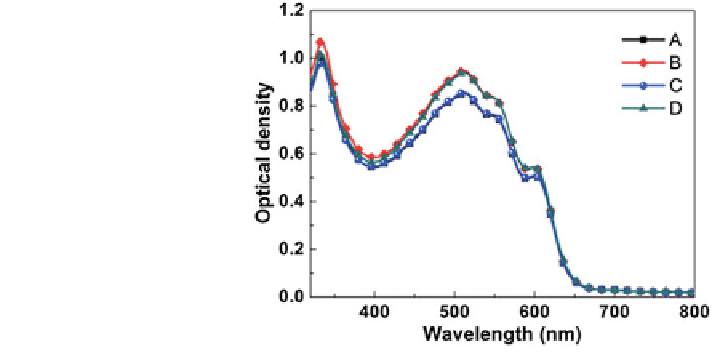
absorption spectrum of the active layer does not show any clear change from the
control Device A as shown in Fig.
8.20
.
This is in good agreement with previous report [
18
], which can be explained by
the finding that the strong near field around Au NPs due to the LSPR distributes
laterally along the PEDOT:PSS layer instead of vertically penetrating into the
active layer. Meanwhile, from the hole mobilities of Devices A and B derived
from the hole-only devices, there is no obvious changes (see Fig.
8.21
), indicating
that charge transport in the bulk of the active layer is unaffected by NPs incor-
porated in PEDOT:PSS. The surface morphology of the PEDOT:PSS ? Au NPs
layer showed an obvious increase in surface roughness with the RMS roughness
increasing from 0.97 to 1.55 nm. Therefore, the incorporation of Au NPs only in
PEDOT:PSS increases the interfacial contact area between the active layer
(P3HT:PCBM) and PEDOT:PSS, allowing more efficient hole collection at the
anode, and hence increases
J
sc
and FF [
23
,
57
]. Furthermore, from resistive
Fig. 8.20 Absorbance of the
active layer for different NP
doping structures [
56
]


Search WWH ::

Custom Search