Environmental Engineering Reference
In-Depth Information
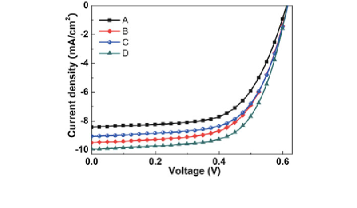
8.4.1 Performances of Au NP Devices
Four device structures have been investigated [
56
] as follows:
Device A: (control): ITO/PEDOT:PSS/P3HT:PCBM/LiF (1 nm)/Al (100 nm)
Device B: ITO/PEDOT:PSS ? Au NPs/P3HT:PCBM/LiF (1 nm)/Al (100 nm)
Device C: ITO/PEDOT:PSS/P3HT:PCBM ? Au NPs/LiF (1 nm)/Al (100 nm)
Device D: ITO/PEDOT:PSS ? AuNPs/P3HT:PCBM ? Au NPs/LiF (1 nm)/Al
(100 nm)
J-V characteristics of the four OSC device structures with Au NPs incorporated
into different organic layers are shown in Fig.
8.19
, and the photovoltaic param-
eters are listed in Table
8.2
.
We observe that the incorporation of Au NPs into either the PEDOT:PSS layer
(Device B) or the active layer (Device C) or improves PCE from 3.16 (control
Device A) to 3.61 and 3.44 %, respectively. Interestingly, the simultaneous
incorporation of Au NPs into both layers results in a further improvement of
average PCE to 3.85 %, which corresponds to *22 % increment from the control
Device A. In all cases, the increases in PCE are results of improvements in J
sc
and
FF, while the V
OC
is unchanged. Notably, when incorporating Au NPs into both
PEDOT:PSS and active layer simultaneously, the series resistance (R
S
) reduces
obviously from 3.05 (Device A) to 1.93 X
cm
2
(Device D), contributing to a
remarkable increase of FF from 61.92 to 65.00 %. To study the origins of PCE
improvement, we first separately study the effects of NPs when incorporated into
either the PEDOT:PSS or P3HT:PCBM layer, which is followed by discussions on
PCE improvement when NPs are incorporated in all polymer layers.
Fig. 8.19 a J-V characteristics of the OSCs with NPs incorporated into different layers under
AM 1.5G illumination at 100 mW/cm
2
[
35
]
Search WWH ::

Custom Search