ABSTRACT
Colloidal crystals were grown on flat or patterned glass slides. The structure of the grains and their defects was first visualized by 3D confocal microscopy and then characterized using simple geometric measurements. Crystals grown on a flat surface maintained a layered structure induced by the closed-packed planes. In the case of the [110] E5 grain boundary, the presence of particles in interlayer position was established.
Introduction
The grain-level microstructure of a material influences a wide range of material properties, including strength, toughness and corrosion resistance. For that reason, understanding and controlling the structure and evolution of grain boundaries is one of the central tasks of materials science. Studying grains at the atomic level moreover, is not an easy task. To aid in this, we used colloidal suspensions as model systems that form crystals. In recent research, colloids have been used to model atomic or molecular systems since they form many of the same phases. They can be used for model glasses as well as crystals [1, 2]. A colloidal system has two distinct phases: a dispersed phase and a continuous one. The dispersed phase consists of small solid particles, on a nano to macro scale, which are dispersed evenly through the continuous fluid phase. The particles used in this study interact as hard spheres. When these particles sediment onto a flat surface, they can form crystals; when they sediment onto an irregular, rough surface, they can form amorphous structures. For the random close-packing, the structural paradigm for the amorphous phase, the volume fraction of solid,f is about 0.63, and for the close-packed crystals, f is about 0.74. The crystals often contain defects and the focus of the present paper is on grain boundaries. The main purpose of the paper is to show how the crystals can be grown and imaged in three dimensions (3D) using confocal microscopy.
Experimental procedure
Colloidal suspension
Silica particles (diameter 1.55 ^m, density 2.0 g/cm3, mass 3.9 x 10⁻¹⁵ kg) were suspended in a water – 62.8 vol. % dimethylsulfoxide (DMSO) solution that matched the index of refraction of the silica and had a density of 1.10 g/cm3. The average velocity of Brownian motion is given by:
where kB is Boltzmann’s constant, T the temperature and m the mass of the particle. For our case, this gives <vB>=2 x 10⁻³ m/s. The gravitational settling velocity of the particle is given by
where VP and r are, respectively, the volume and radius of the particle, Ap is the density difference between particle and fluid, and n is the viscosity of the fluid, which is about 10-2 Pa.s. This gives in our case vs=10-6 m/s, which satisfies the condition for a colloidal systems (vB>>vs). The index match makes the system optically transparent, which allows investigation by optical confocal microscopy at large distances into the sample. Contrast between particle and solution was achieved by adding fluorescein dye to the solution. The index match also minimizes the van der Waals forces between the particles, which interact therefore like hard spheres.
Template
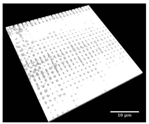
The crystal growth can be controlled by slowing down the sedimentation of the colloids (described above) and the use of a template. The controlled growth of the layers was achieved by diluting the initial suspension by a factor of two. A template is a patterned substrate that directs the setting of the particles in such a way that the structure, orientation, and size of the crystal is pre-determined. This process is called "colloidal epitaxy."[3] The templates were fabricated in the following way. A positive mask of the targeted pattern (set of holes) was first printed on a chrome-coated substrate (chrome was removed using a Heidelberg™ mask maker). A thin layer of photoresist was then spin coated on a primer-coated glass slide (the subsrate) and polymerized (3 minutes at 110°C). This assembly was then exposed using a mask aligner (SussTM) for 2-2.5 sec. The time varied depending on the size of the holes in the chrome mask, the age of the photoresist, calibration of the mask aligner, and the premixed developer. The slides were then developed for 60 to 90 sec in a photoresist developer (mixture of 1 part of MF351 and 5 parts water). The silica was then etched in a reactive ion etcher (RIE). The plasma needed to be stable before the sample was inserted into the clean chamber. The reactive ion etching ran for about 10 minutes. Finally, to remove the remaining photoresist layer, the sample was exposed tin the same RIE to an oxygen cleaning plasma, which cleans the photoresist without etching the silica. An example of the resulting template, imaged by confocal microscopy, can be seen in Figure 1. In this example template, we have attempted to etch holes with a gradient of sizes.
Figure 1 : Confocal image of a pattern etched in a silica glass microscope slide (the white phase is the glass). The pattern has holes of different diameters.
Confocal microscope
In a laser scanning confocal microscope, [4] light is focused through a microscope objective where it excites fluorescence in the sample. The emitted light is retraced through the microscope and passed through a pinhole in the conjugate focal plane of the lit spot in the sample. This allows only light from that spot to pass; light from all other directions, for example from multiple scattering or fluorescence, is blocked. The light intensity is recorded by a detector and stored as the spot is scanned through volume of the sample. The stored information can then be displayed directly as a three-dimensional image or be processed into a reconstructed image, in which computer graphics is used to redraw the spheres.
When the refractive index of the fluid is matched to that of the spheres, light can penetrate quite deeply into the sample with little scattering, so that tens of planes of a crystal can be imaged. The lateral resolution (perpendicular to the optical axis) is about 200 nm, typical for optical microscopy. Because of limitations of the optics, the vertical resolution is only 500 nm. Application of image analysis techniques [5, 6] improves the resolution for the location of the center of the particles by about an order of magnitude. A typical time to scan a stack of planes through a sample is a few seconds.
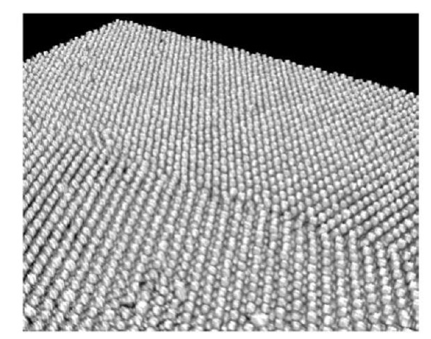
Figure 2 (a) and (b) show a crystal imaged using this technique and presented in the form of gray-level confocal images. Fig. 2(a) shows an x-z plane, orthogonal to the x-y plane shown in Fig. 2(b). These images are numerically extracted from the 3D data set recorded in the confocal microscope. Note that this data set is collected by acquiring 2D images (x-y images in the reference of the microscope) such as Figure 2(b). These are roughly parallel to the plane of the glass substrate. The acquisition is repeated by scanning along the third perpendicular direction, z, aligned with gravity. The spacing along the z plane is chosen to be equal to the pixel size in the x-y plane so that the stacking of these images is an isotropic reconstruction of the 3D structure of the crystal. The imaged crystal was grown along the z direction onto an etched glass pattern of a [100] E5 grain boundary. The location of the grain boundary is indicated by a dark line in figure a). In Figure 2(b), extracted right at the middle plane of the first layer of deposited particles, the grain boundary is clearly visible. A white line has been drawn to indicate the location where Figure 2(a) was extracted. Figure 3 is a 3D rendering of the same data set after binarization by thresholding the particles and applying 100% transparency to the voxels located in the liquid phase.
Figure 2 : Two gray-level confocal images (slices) of a [100] E5 bi-crystal grain boundary grown on a etched silica template. (a) x-z slice; (b) x-y slice. The location of the grain boundary is indicated by a dark vertical line in figure (a). It is clearly observable in figure (b), which is taken at the level of the first layer of particles, just above the glass pattern. The light gray line in figure (b) shows the location of (a).
Figure 3 : Grazing incidence view of a 3D rendering of the bi-crystal shown in Figure 2. The diameter of the silica particles is 1.55 ^m.
Results and discussion
Structure of columnar polycrystals on a flat glass slide
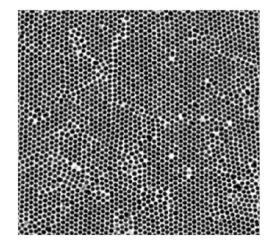
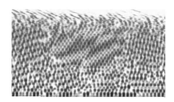
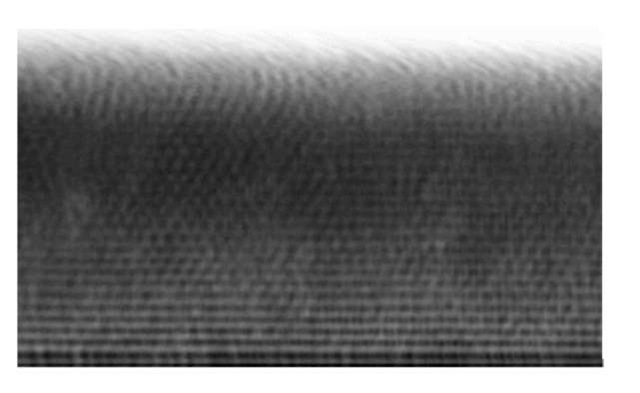
When setting slowly on a featureless flat glass slide, the colloidal particles spontaneously form crystals by successive deposition of hexagonal close-packed planes. Crystals nucleate in several places with random orientations and grow into grains, separated by grain boundaries. Two different polycrystalline samples were grown using this procedure. The first was grown using a small amount of solution in the container, while the other one was grown using three times this amount. This resulted in two samples with different thickness. Figure 4 shows an x-y plane of the thin sample. It reveals the polycrystalline nature of the deposited crystals. The thin sample had only 9 deposited layers and the structure is rather well preserved all through the thickness. Note that the image also reveals vacancies and defects in the form of agglomerated particles. Figure 5 shows a x-z slice of the thick sample. In this direction again the different grains can be observed, with the structure becoming more disordered as the distance from the substrate increases. Figure 6(a) and (b) again, show the typical structure of these two crystals observed in the x-z direction, but to account for the total volume analyzed, the gray level was averaged along the entire third perpendicular direction (y) and projected onto the 2D images. This averaging clearly highlights the order of the structure along the z direction, in the form of the successive close-packed planes. It also shows that since the sample is imaged from the bottom, the quality of the images is decreases when the distance to the substrate increases because of increasing scattering of the light perhaps due to imperfect index matching.
Figure 4: Confocal imaging of a layer of a thin polycrystalline sample close to the deposition surface.
Figure 5 : Confocal view of an x-z cut of a thick polycrystalline sample showing the different grains. The structure becomes more disordered at a larger distance from the substrate.
Figure 6 a). x-z view of the thin sample. The intensity is averaged over the entire third perpendicular direction (y), to form a projection.
Figure 6 b). x-z view of the thick sample. The intensity is averaged over the entire third perpendicular direction (y), to form a projection.
E5 grain boundary
The structure of the E5 boundary shown in Fig. 2-3, is analyzed in more detail here. The bi-crystal consists of only four deposited layers (see Fig. 2(a)). Figure 7 shows the first layer of this model grain boundary. The two superimposed sets of lines show what the grain boundary structure should be if each hole in the pattern was filled with a particle as described in [7]. The atom on the left marked with an arrow is shared between two possible sites which can be considered as a defect. The set of white arrows point atoms which are present while they shouldn’t according to the model created for this grain boundary. Figure 8 shows a 3D rendering of the position of these atoms replotted after the determination of the position of their center of gravity. In this figure, the atoms are colored according to the value of their distance to the substrate z. All the small blue points are located in layers. The larger colored points (red, yellow and green) have been determined -thanks to their value of z- as being in interlayer positions. The figure shows that, apart for some defects, a lot of atoms in these interlayer position are located close to the grain boundary which is in the plane located at x=12.5 microns and is indicated by a dashed line in the Figure.
Figure 7 : Structure of the [100] £ 5 grain boundary. The black arrow on the left indicates a location where a single atom is present where there should be two sites. The white arrows show sites where atoms are present at places they should not be in the ideal £5 hard sphere structure. [7]
Figure 8 : 3D view of the position of atoms as seen from the side of the grain boundary. The large atoms are in interlayer positions. Apart from a few defects, most of the interlayer atoms are located at the grain boundary which is in the plane defined at x=12.5 microns indicated by the dashed black line.
Conclusions and perspective
This paper shows some 3D images of grain boundaries in colloidal crystals grown on glass microscope slides. The particles are silica spheres, monodisperse with a diameter of 1.55 ^m. When deposited on a flat surface, grain boundaries form due to the aggregation of the particles in the form of close-packed planes. The successive deposition of close-packed planes is preserved over a long distance from the substrate, but a side view of a tall sample shows that the grain structure become more and more disordered. The paper also shows that colloidal epitaxy of bi-crystals is feasible, as exemplified in the case of a [100] E5 grain boundary between two face-centered cubic crystals. The boundary contains atoms in an interlayer position. Future work will focus on the study of the mobility of the atoms at these grain boundaries.

![Two gray-level confocal images (slices) of a [100] E5 bi-crystal grain boundary grown on a etched silica template. (a) x-z slice; (b) x-y slice. The location of the grain boundary is indicated by a dark vertical line in figure (a). It is clearly observable in figure (b), which is taken at the level of the first layer of particles, just above the glass pattern. The light gray line in figure (b) shows the location of (a). Two gray-level confocal images (slices) of a [100] E5 bi-crystal grain boundary grown on a etched silica template. (a) x-z slice; (b) x-y slice. The location of the grain boundary is indicated by a dark vertical line in figure (a). It is clearly observable in figure (b), which is taken at the level of the first layer of particles, just above the glass pattern. The light gray line in figure (b) shows the location of (a).](http://what-when-how.com/wp-content/uploads/2011/07/tmp11103_thumb_thumb.jpg)

![Structure of the [100] £ 5 grain boundary. The black arrow on the left indicates a location where a single atom is present where there should be two sites. The white arrows show sites where atoms are present at places they should not be in the ideal £5 hard sphere structure. [7] Structure of the [100] £ 5 grain boundary. The black arrow on the left indicates a location where a single atom is present where there should be two sites. The white arrows show sites where atoms are present at places they should not be in the ideal £5 hard sphere structure. [7]](http://what-when-how.com/wp-content/uploads/2011/07/tmp11109_thumb_thumb.jpg)

