INTRODUCTION
The ongoing miniaturization in size and integrity of electronic and mechanic devices has led to an interest in fabrication of nanometer-sized uniform structures on surfaces. With the device downscaling dimensions to the nanometer range, current interest is focused on the state-of-the-art lithographic development such as electron beam lithography, extreme UV lithography, imprint lithography, and scanning probe microscope (SPM) lithography. Binnig et al.[1] first developed the scanning probe microscope in 1982, and since then, SPM have been primarily used to obtain topographic and electronic surface maps. Nowadays, SPM is also being used to fabricate patterns and structures in nanometer scale, as well as to directly modify chemical or physical structure of surfaces.
Among several nanolithographic methods, scanning probe lithography (SPL) is one of the best lithographic techniques for forming nanostructures. Scanning probe lithography using a sharpened tip of an atomic force microscope (AFM) or a scanning tunneling microscope (STM) with the highest spatial resolution has demonstrated outstanding capabilities for atomic-level manipulation, and also wide varieties of potential applications such as electronic devices,[2'3] biochips, and biosensors1-4’5-1 using different approaches—a direct method of writing patterns consisting of relatively small molecules on solid state surface, an exposure of organic thin films such as self-assembled monolayers (SAMs) and a selective anodic oxidation of various substrates. In particular, AFM lithography is the most promising method for fabricating organic thin films or the substrate itself in nanometer scale. Whereas STM-based lithography is mainly carried out in ultrahigh vacuum (UHV), fabrication using AFM lithography can be performed in liquid state as well as in ambient environment. Also, several novel methods using AFM as a lithographic tool have been developed in the past 10 years. This is a very active research area because of the flexibility and simplicity of the technique. In this technique, an AFM tip may be used to carry catalysts to selectively induce surface reactions, to attach molecules on surfaces as a pen, and to direct local oxidation on surfaces as an electrode.
Subsequently, several principal AFM nanolithography techniques on organized molecular films such as self-assembled monolayers, Langmuir-Blodgett (LB) monolayer, and spin-coated polymer films will be illustrated.
AFM-BASED NANOLITHOGRAPHY
Dip-Pen Nanolithography
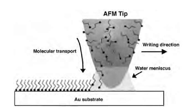
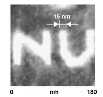
Mirkin and coworkers1-6,7-1 introduced a dip-pen nanolithography (DPN) to construct patterns of molecules on a substrate in a positive printing by using an AFM tip as a ”pen,” Au substrate as a ”paper,” and alkanethiols with chemical affinity for Au substrate as ”molecular inks.” In DPN, molecules are moved from the AFM tip to the solid substrate via capillary action to perform nanoscale patterns directly. The schematic diagram of patterning process in a DPN is shown in Fig. 1, and Fig. 2 represents the nanopatterns of alkanethiol on gold substrate via DPN.
Although DPN resolution relies on some parameters such as grain size of Au substrate, the contact time of tip-substrate, and relative humidity, this technique is a simple method for transporting molecules from AFM tip to substrate to control the architecture of a surface on the sub-100 nm.
Recently, DPN has been improved to generate nano-array with dot-and-line pattern of biomolecules such as proteins, oligonucleotides, and magnetic nanoparticles. In case of fabricating magnetic nanostructures, 16-mercap-tohexadecanoic acid (MHA) is used to make nanopatterns on Au substrate via DPN at the first stage, and then this patterned Au substrate is dipped into 1-octadecanethiol solutions to form passivated layer. Then, this sample is immersed into the iron oxide nanoparticles suspension solution once more. After going through these procedures, nanoarray with almost identical magnetic dots and lines composed of nanoparticles is prepared.1-8-1
To investigate a various surface-mediated biological recognition phenomenon, the construction of biomaterial nanoarray is needed. DPN is useful not only to fabricate nanopatterns for differentiating active area from nonspecific binding site of the substrate, but also to recognize specific binding properties. DPN forms nanopatterns on Au substrate using alkanethiols coated on AFM tips, and initially, the system of organothiols-gold substrate was used to fabricate nanopatterns because it was simple to use. However, the electrical conductivity of the gold substrate interferes with the observation of charge transport and near-field optical properties in building up nanostructures on surfaces like this, and also quenches the emission from any surface-bound materials with fluorescence.1-9,10-1 Thus oxidized silicon substrate, as well as gold substrate, are used to generate nanoarray of proteins, oligonucleotides. In the case of oxidized silicon wafers as substrate, there are two ways to modify the substrate to form nanoarray through DPN. One is to charge the silicon oxide surfaces negatively by treatment of base, and the other is to modify the surface with aldehyde functional group. AFM tip is modified by organosilane that forms a biocompatible and hydrophilic surface layer. Next, proteins are attached to the modified silicon oxide surface via DPN with AFM tip coated by immersing the tip in protein solution because of electrostatic interaction between the positively charged sites of the proteins and the negatively charged surface or covalent bonding between the surface with aldehyde functional head group and amine group on the proteins.[11] In a similar manner, DPN can be extended to useful direct-write methods to fabricate nanoarray of proteins using silicon oxide substrate and gold substrate.
Fig. 1 Schematic representation of DPN. A water meniscus forms between the AFM tip coated with alkanethiol and the Au substrate.
Nanografting Lithography
Liu and coworkers[12-14] have reported the nanografting technique for fabricating a patterned self-assembled monolayer (SAM) by combining mechanical displacement of selected molecular resist by an AFM tip and backfilling of new adsorbates.
In this case, SAM alkanethiol molecules at selected areas of the gold surface are removed by an AFM tip with a force greater than the threshold displacement force to fabricate desired patterns within the SAM. Next, new alkanethiol molecules having different alkyl chains from the contacting solution are immediately adsorbed onto the exposed regions by an AFM tip. Fig. 3 shows the procedure for the nanografting lithography.
Using nanografting, the fabricated patterns can be quickly obtained in situ without changing the mask or repeating the entire fabrication procedure.
A nanopen reader and writer (NPRW), an improved nanografting technique, was introduced to produce nano-patterns on gold surface.[15] This technique combines the advantage of both nanografting and DPN. Compared to the existing nanografting technique, the NPRW technique has several advantages. In contrast to DPN, the resolution of NPRW is not influenced by the texture of the paper and the humidity of the experimental surroundings. Also, nanopatterns are easily fabricated and characterized in both solution and ambient environments, as well as solution phase in NPRW experiments. This technique is useful for producing nanopatterned arrays of biomolecules such as DNA and proteins.[16-18]
Constructive Nanolithography
More recently, nanopatterning techniques using applied bias between the scanning probe microscope tip and the sample were reported. Sagiv and coworkers suggested a constructive nanolithography[19-21] that can be adapted to construct hybrid metal-organic nanostructures on silicon surface. In the constructive nanolithography, an electrically conducting AFM tip composes nondestructive chemical information on the exposed outer surface of self-assembled monolayers, and converts modified surface into a nanopatterned template for spatial control of the surface self-assembly of various selected organic and inorganic nanostructures.
Fig. 2 Nanoscale molecular letters written on an Au(111) surface with 16-mercaptohexadecanoic acid (MHA) molecules by DPN.
Fig. 3 Schematic diagram of the nanografting process.
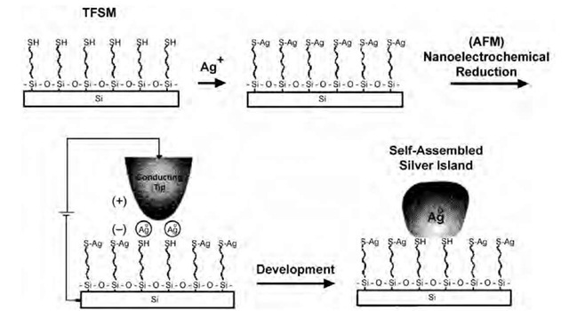
Metallic silver nanoparticles are generated at selected surface regions by AFM tip-induced electrochemical reduction of the surface-bound metal ions on a thiol-top-functionalized silane monolayer (TFSM).[19] They also take the shape of the organic bilayer template on spatially modified,[20] nondestructive n-octadecyltrichlorosilane (OTS) SAMs via an electrically biased AFM tip, and then build various inorganic particle or layer. The scheme of constructive nanolithography is summarized in Fig. 4.
Nanolithography Using Current Sensing AFM
Zhao and Uosaki[22,23] prepared well-defined nanopatterns of alkanethiol SAMs on gold substrate by using current sensing atomic force microscopy (CS-AFM). When the conducting tip with a sufficient bias was scanned over a SAM in inert solvent containing alkanethiols with different chain length, the original SAM underneath the tip was removed and a new nanometer-sized spatial SAM of the alkanethiol was formed. In this method, toluene was chosen as the medium because of its nonpolarity and low dielectric constant. A leak of current can be avoided, and the amount of water contained in toluene also has a crucial effect on lithographic performance. The mechanism of CSAFM-based lithography is as follows:
For positive bias condition,
For negative bias condition,
Anodization AFM Nanolithography
Some AFM-based nanolithographic methods are not practical because their lithographic speed is only in the order of nanometer/second, and both nanografting and current sensing AFM lithography are usually accomplished under liquid-solid interface.
Fig. 4 Scheme of the constructive nanolithography: the site-defined self-assembly of silver metal on a thiol-top-functionalized silane monolayer preassembled on silicon.
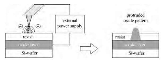
Fig. 5 Schematic description of AFM anodization nanolithography on silicon substrate.
However, the anodization lithographic technique, one of the most promising methods to prepare nanopattern with AFM, is accomplished by the reaction on the substrate surface.
AFM anodization lithography has also been reported elsewhere for producing protruded oxide patterns on a substrate by faradaic current from the cathode tip to the anode substrate.[24-37] Anodic patterning can be mainly accomplished on silicon[33,34- or titanium substrate[38,39- by electrochemical reactions mediated by the scanning probe tip. Electrochemical anodization occurs by emitted electrons from the tip at the locally scanned area on a silicon substrate in the presence of an atmospheric water column between the tip and the scanned area of the sample. This direct modification of silicon or metal surfaces by the anodization process using the electric field from an AFM tip is one promising method of accomplishing direct-writing lithography for the electronic device fabrication.
The first report of tip-induced oxidation of silicon was the STM study by Dagata et al.[40] They used an H-pas-sivated silicon surface with a positively biased tip for generating oxide features on the surface. They suggested that the electrochemical oxidation reaction, which is locally induced beneath the tip in an adsorbed water column on the sample surface, is responsible for metal and semiconductor surfaces.
As shown in Fig. 5, the emitted electrons flow from the tip to the substrate through an organic resist, and they cause the anodization process with water on the silicon substrate. Accordingly, a protruded oxide pattern is newly formed at the local area of the substrate as a result of the anodization process.
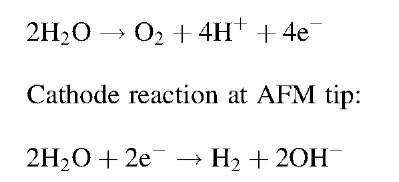
Sugimura and Nakagiri[25- have suggested an electrochemical reaction between the tip and the sample for the anodization lithography as follows:
Anode reactions at sample surface:
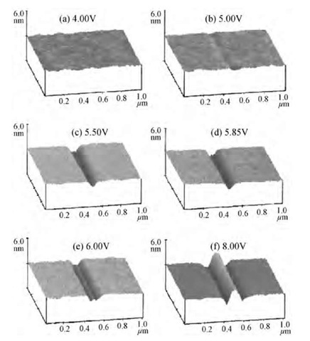
As the AFM anodization nanolithography is closely related to the magnitude of current, the size of the protruded pattern strongly depends on the amount of accepted electrons on the substrate. Also, it has been reported that the geometric factors of the nanopattern, such as the protruding height and the line-width, are affected by scan [26,33,37,38- speed or duration time of the cathode AFM tip,[26,33,37,38- [30,34,35,37- surface group, environmental relative humidity,[ ,,,] and the applied voltage between the tip and the sam-ple.[33,34- Even the operational mode of AFM, both contact mode and noncontact mode, also influences on anodization pattering.[41]
The key to reach high resolution and precision is to selectively modify the surface either by breaking chemical bonds or through direct chemical reactions using local tip-surface interactions. The selection of high-performance resist materials is one of the important factors in the successful application of AFM lithography.
In the case of resist, the resist film should be prepared in a thin and uniform layer to attain high resolution in nanometer scale. Langmuir-Blodgett (LB) films[28,29,42- and self-assembled monolayers’-27,30,43-46-1 have been used as resists and patterned with nanometer precision. These films are well-organized molecular assemblies formed by layer-by-layer deposition via either van der Waals force or covalent bonding.’47- The size of the molecule determines the layer thickness and can be carefully controlled to produce layers of uniform coverage. SAM films, consisting of organosilane, bipolar amphiphiles, and al-kanethiol molecules, show a great potential as ultrathin resist films. Such SAM films, formed through the chem-isorption onto oxide and metal surfaces, have excellent uniformity in molecular order and resistivity to various types of chemical reagents. As most of the lithographic works with organic resists have been exclusively carried out on silicon surface for practical application, several organic resists with different functional groups have been studied in order to investigate the surface group effect on the anodic anodization using AFM.
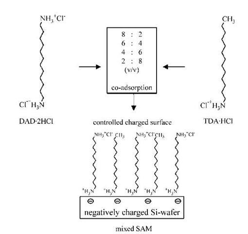
Fig. 6 Preparation of the mixed SAM of DAD and TDA on a negatively charged Si wafer.
Fig. 8 Lithographic pattern at constant lithographic speed at the specified voltage: (a) 4.00 V, (b) 5.00 V, (c) 5.50 V, (d) 5.85 V, (e) 6.00 V, and (f) 8.00 V.
