INTRODUCTION
Novel nanofabrication techniques are being explored as alternatives to conventional lithographic techniques to mass produce structures with feature sizes smaller than 100 nm and to minimize costs.[1] Porous anodic aluminum oxide (AAO) is a self-ordered, hexagonal array of straight cylindrical pores with high densities (108-1011 pores/ cm2), tunable diameters (5-250 nm), and depths (a few nanometers to hundreds of micrometers).[2-5] It can be fabricated through electrochemical anodization of aluminum at moderate and constant temperatures of 0-10°C in aqueous acidic electrolytes.[6-8] Anodic aluminum oxide is optically transparent in the fingerprint UV/vis and IR regions[9] and thermally stable up to 1000°C.[1O] Moreover, it has recently been demonstrated to have unique advantages in several technological applications, including nanotemplating,[3,4] membrane transport,[11] and photonic crystals.[12] Through-hole AAO membranes have been used as evaporation masks to fabricate nanodot arrays[13,14] and as etching masks to transfer patterns into several substrates including diamond,[15] silicon,[16,17] and other semiconductors.1-18-1
The high fragility of through-hole AAO membranes[19] limits their integration into established microfabrication processes where robust membranes are needed. Although an elastic polypropylene support ring that runs around the circumference of AAO membrane permits one to pick up the membrane with membrane tweezers without shattering the membrane,1-20-1 this approach fails when the membrane undergoes a high-temperature and/or an ultrahigh vacuum. To provide additional supports to fragile AAO, one could pattern aluminum surfaces with an anodization barrier prior to anodization. During anodization of the patterned surfaces, the anodization barrier prevents anod-ization in the patterned areas while the oxide grows in the unpatterned areas. Recently, Huang et al.[21] have reported the first anodization barrier of polymethylmethacrylate deposited on aluminum films. Because of the penetration of the electrolyte through this polymeric layer, the underlying surface was partially anodized to form AAO up to 10-nm deep. In addition, the procedure required optical lithography, polymer nanoprinting, ion-beam exposure, and milling. Because of its excellent adhesion to aluminum surfaces and electrical insulation as well as its inertness to acidic electrolytes,[22] a SiO2 layer pre-patterned on aluminum surfaces could provide a good anodization barrier. The patterning of aluminum surfaces with a SiO2 layer can be achieved through a sol-gel coating or a dielectric evaporation.
This paper describes a patterned anodization of bulk aluminum sheets and evaporated aluminum films pre-patterned with an anodization barrier of SiO2 through a sol-gel process or a dielectric evaporation. Using a two-step anodization process,[6-8] we formed highly ordered, uniform, and straight nanopores of AAO in the unpat-terned areas, and did not observe any pores in the patterned areas before and after SiO2 was removed. This approach provides intermittent aluminum supports to fragile AAO membranes, allowing facile incorporation of AAO in a robust form into microdevices for microelectronics, microfluidics, and integrated optics.
ANODIZATION CELL
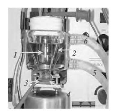
In most of the reported anodization processes, the whole aluminum sheet has been exposed to the anodizing electrolyte to fabricate ordered AAO. This results in a complete conversion of an aluminum surface into fragile AAO, and thus limits the integration of AAO into mi-crofabrication technologies that require robust AAO at specifically defined sample areas. To address this issue, Li and Metzger[23- coated one side of aluminum sheet with an insulating layer. To further address this, we prepared a custom-built novel anodization cell and used it in our experiments (Fig. 1). This jacketed cell is specifically designed for general temperature-controlled electrochemical experiments where film and/or membrane electrodes are used, and is compatible with a commercially available cell stand (BAS Inc., Indiana). The samples to be anodized, aluminum sheets or vacuum-evaporated aluminum films on glass slides, serve as the anode. The anode is clamped down against a Teflon-coated rubber O-ring in the anodization cell. Another piece of aluminum sheet serves as the cathode. Alligator clips are used to connect the power supply to the electrodes.
Fig. 1 Custom-built anodization cell: (1) aluminum cathode; (2) thermocouple thermometer; (3) aluminum anode; (4) Teflon-coated O-ring; (5) water inlet; and (6) water outlet.
PATTERNED ANODIZATION ON BULK ALUMINUM SHEETS
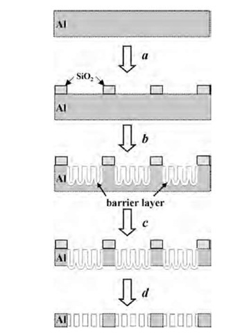
Scheme 1 shows our procedure to fabricate freestanding and through-hole AAO membranes with intermittent aluminum supports on bulk aluminum sheets. Sol-gel coatinga or dielectric evaporation forms the SiO2-pat-terned surfaces. The patterned surfaces were anodized using a two-step anodization process as previously des-cribed.[6-8] Briefly, the patterned surface was degreased in a 5 wt.% sodium hydroxide solution at 60°C for 30 sec, neutralized in a 50% (wt/wt) nitric acid solution for 5 sec, and then rinsed with deionized water. The pretreated surface was first anodized at a voltage of 40 V in a 0.3 M oxalic acid solution at 0°C for 20 min to eliminate large ridges and to texture the surface. The oxide was removed in a mixed solution of 0.2 M chromic acid and 0.4 M phosphoric acid at 60°C for 5 min. The surface was then anodized for 2 hr to create long-range ordering, with the newly formed oxide being removed again under the same conditions as used in the first anodization. Finally, the thus-treated surface was anodized again under the same conditions for 30 min to grow highly ordered pores. The postetching treatment of the resulting AAO consists of three steps: 1) removal of the remaining aluminum in a saturated mercury(II) chloride solution; 2) removal of the barrier layer at the bottom in a 5 wt.% phosphoric acid solution at 30°C; and 3) removal of the patterned SiO2 on the top in a 5 wt.% sodium hydroxide solution at room temperature.
Aluminum sheets (99.999%, 0.25-mm thick) were purchased from Aldrich. Before use, they were cut into small pieces (20 x 20 mm). The SiO2 sol used for patterning was prepared by adopting a two-step, acid-catalyzed sol-gel process. In a typical preparation, tetraethyl-orthosilicate (TEOS), ethanol, deionized water (18.2 MO cm) and dilute hydrochloric acid solution (HCl) were mixed in a molar ratio of 1:3.8:1:0.0005. The resulting solution was refluxed at 60°C for 90 min to provide the stock sol. Before use, 1 mL of stock sol was diluted with ethanol, followed by addition of water and dilute HCl solution, to provide a final overall molar ratio of TEOS/ ethanol/water/HCl to be 1:22:5:0.0053. The SiO2 sol was introduced into Marsmatic technical pens (0.13-mm tip, Staedtler) and was used to pattern the aluminum sheets.
Scheme 1 Schematic diagram for the micropatterning process of aluminum foils through a sol-gel resist. (a) Micropatterning of anodization barriers using various techniques including microwriting, screen printing, and chemical vapor deposition; (b) patterned anodization; (c) removal of the remaining aluminum in a saturated mercury(II) chloride solution; (d) removal of the barrier layer at the bottom in a 5 wt.% phosphoric acid solution and removal of the patterned SiO2 on the top in a 5 wt.% sodium hydroxide solution.
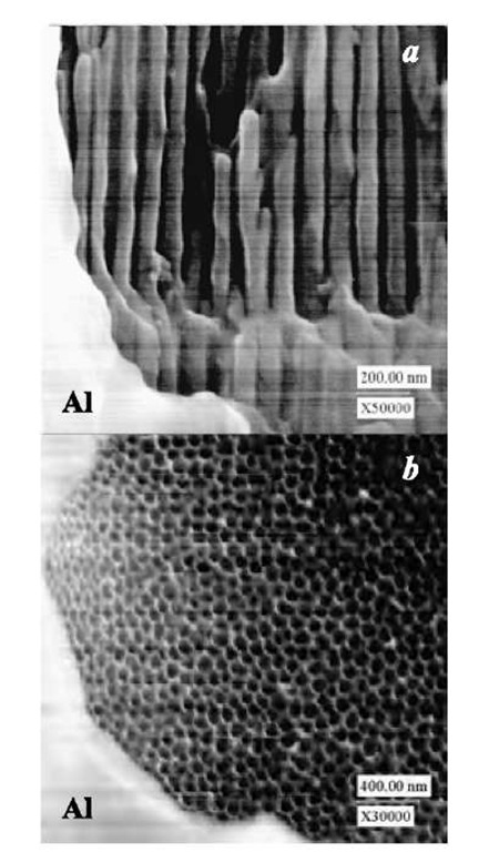
Fig. 2 Scanning electron micrographs of ordered AAO on an aluminum sheet prepatterned with SiO2 circular spots (ca. 1-mm diameter) through a sol-gel process: (a) cross-sectional view of the AAO / Al interface; (b) surface view of the AAO / Al interface. b was obtained by dissolving SiO2 in a 5 wt.% sodium hydroxide solution.
Fig. 2a shows an illustrative scanning electron microscope (SEM) cross-sectional micrograph of AAO on a bulk aluminum sheet prepatterned with SiO2 circular dots (ca. 1-mm diameter). Highly ordered, uniform, and straight pores are evident in the unpatterned areas. The average pore diameter, depth, and density are determined by SEM images to be 43±7 nm, -10 mm, and 1.7 x 10¹⁰ pores/cm2, respectively. No pores appear in the areas beyond the O-ring, indicating no electrolyte leak from the inside to the outside of the O-ring. No pores are observed in the patterned areas. Appearing visible as a thin overhang around the periphery of the AAO membrane, the patterned SiO2 layer shows no cracking and/or peeling against the applied voltage and anodizing electrolytes. Shown in Fig. 2b, no pores are observed beneath the SiO2 layer if it is removed using a 5 wt.% sodium hydroxide solution at room temperature for 5 min. The pores were also widened to be about 60 nm as a result of base etching. This demonstrates an excellent inhibition of the SiO2 layer in preventing the electrolyte from penetrating into the SiO2 / aluminum interface. The inhibition ability of the SiO2 layer, together with the good adhesion to aluminum and the capability of undergoing long-time anodization, makes SiO2 an ideal resist for patterned anodization of aluminum.
After carefully removing the remaining aluminum, the bottom-barrier layer, and the patterned SiO2 layer, a freestanding, highly ordered, through-pore AAO membrane with intermittent aluminum supports is obtained. In our control experiments, we anodized patterned aluminum sheets under the same conditions, except for the different anodization times in the final step (from 30 min up to 11 h). We then measured the membrane thickness by SEM for the resulting freestanding and through-hole AAO membranes. We found that the membrane thickness increased almost linearly with the anodization time in the final step up to 9 h, after which it increased slightly with the anodization time in the final step. For example, the membrane thicknesses are 13.2± 1.3, 23.6±0.4, and 24.3±0.4 mm for a 5, 9, and 10 hr anodization in the final step, respectively, with the aspect ratio of the nanopores in the membranes being 307±58, 549±90, and 565 ±92, respectively. Because the pH value of the electrolyte mainly defines the nanopore diameter,[26] during the two-step anodization process in a given poly-protic acid, the nanopore diameter is held almost constant. One can control the anodization time in the final step to control the depth of the nanopores. This offers a unique advantage to tailor the aspect ratio of the nanopores. Huang et al.[21] found that sub-100-nm AAO pores with aspect ratios 1000:1 can easily be formed without elaborate processing.
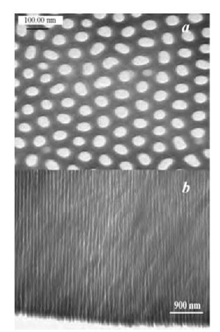
Fig. 3 Transmission electron micrographs of surface (a) and cross section (b) of freestanding and through-hole AAO membranes.
Fig. 3 shows the transmission electron microscopic (TEM) surface (a) and cross section (b) of a cutout of the freestanding and through-hole AAO membranes. Highly ordered, uniform, and hexagonal pores are evident in Fig. 3a. The average pore diameter became larger than that shown in Fig. 2a. This is because of the pore widening from the phosphoric acid solution used to remove the bottom-barrier layer. Through-hole nanopores oriented normal to the aluminum surface are also clearly shown in Fig. 3b.
ANODIZATION ON EVAPORATED ALUMINUM FILMS ON GLASS
Although irregular pore arrays of AAO were obtained through a single-step anodization process of bulk aluminum foils at the beginning of 1950s,[27- regular pore arrays were not fabricated until 1995 when Masuda and Fu-kuda[6- demonstrated that a two-step anodization process can dramatically improve the periodicity of the pores. During the past several years, almost all reported works have been using bulk aluminum instead of thin aluminum films. This greatly limits the integration of AAO into potential technologies because of the inherent fragility of AAO membranes[19] and the practical need of many technologies to have materials in thin-film forms. Very few reports are available on anodization of vacuum- [13,17,21,28,29- evaporated aluminum films,[ ,] in which single- step anodization processes with short anodization times (5-13 min) were used, resulting in a low ordering of pore arrangement. To improve the ordering of the pore arrangement, one should use the two-step anodization process with longer anodization times, as for bulk aluminum foils.[30]b To the best of our knowledge, there has been no report on the application of two-step ano-dization process to the evaporated aluminum films.
Fig. 4 Scanning electron micrographs of surface (a) and cross section (b) obtained on vacuum-evaporated aluminum films on glass.
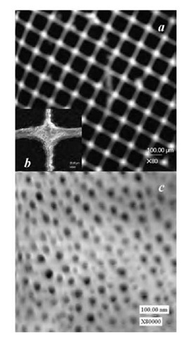
Fig. 5 Scanning electron micrographs of the surface of ordered AAO on an evaporated aluminum film prepatterned with SiO2 microgrids (75 x 75 mm): (a) low-magnification image; (b and c) high-magnification images.
Thin aluminum films (~ 2.2 mm) were obtained by electron beam evaporation of 99.99% aluminum at a rate of 2.0 nm/sec in a vacuum of 2x 10"7 Torr on microscopic glass slides (Baxter Scientific, M6145). The glass slides were cleaned in freshly prepared ”piranha solution” (7:3 concentrated H2SO4 and 30% H2O2), thoroughly washed with water, and blown dry with nitrogen. The films were stored under vacuum in a drying chamber or were immediately used.
Prior to use, the aluminum film was degreased by sonicating in ethanol for 10 min, and blown dry under a stream of nitrogen. The two-step anodization process that was established for bulk aluminum[6-8] was used to anodize aluminum films. Typically, the film was first anodized at a voltage of 40 V in a 0.3 M oxalic acid solution at 0°C for 15 min to texture the surface. After removing the oxide in a mixed solution of 0.2 M chromic acid and 0.4 M phosphoric acid at 60°C for 5 min, the surface was anodized again for 15 min to create long-range ordering. The newly formed oxide was removed again under the same conditions as used in the first anodization. Finally, the thus-treated surface was anodized under the same conditions to grow highly ordered pores. The final anodization was stopped at a point when the anodizing current significantly dropped. At this point, all the aluminum is consumed. For a — 2-p.m-thick film, the anodizing time in the final step is usually about 12 min.
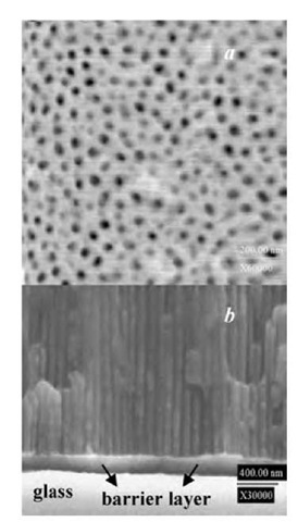
Using the two-step anodization process, we repeatedly observed a circular disk of oxide (ca. 8-mm diameter) locating in the center of the area defined by the O-ring (12-mm diameter). No oxide was present beyond this disk. Huang et al.[21] observed similar delamination behavior. They attributed it to the stress generated as a result of volume expansion when aluminum is anodized to porous alumina. Depositing an adhesion layer between aluminum and glass substrates may eliminate delamination. Fig. 4a shows a scanning electron microscope (SEM) surface micrograph of AAO obtained on the central disk. Highly ordered, uniform, and straight pores can be seen. The average pore diameter, depth, and density are determined by SEM images to be 60±8 nm, — 3 mm, and 1.3 x 10¹⁰ pores/cm2, respectively. This membrane thickness results in a volume expansion of alumina to aluminum of about 1.3, which is in good agreement with the mechanical stress model[31,32] and the 10% porosity rule.[26] Fig. 4b shows the SEM cross-sectional micrograph. There is a thin oxide barrier layer on which parallel, straight-through pores are evident. There are voids of alumina below the barrier layer. Similar voids were previously observed for anodization of aluminum thin films on silicon,[13,17] with the formation being attributed to a localized temperature increase or electric-field-enhanced dissolution near the interface. Because of this unique structure, the bottom part of the oxide layer can be easily removed by postetching treatment with phosphoric acid solution. This allows for the alumina to be directly used as an etch mask for pattern transfer into other substrates.[17]
PATTERNED ANODIZATION ON EVAPORATED ALUMINUM FILMS
The SiO2 pattern (—4.0-p.m thick)c was dielectrically deposited on the freshly evaporated aluminum films on glass at a rate of 2 A/sec by electron beam evaporation at a base pressure of 1.5 x 10~ 5 Torr, using a TEM copper grid (75 x 75 mm) as an evaporation mask. The thus-patterned surfaces were anodized using the two-step anodization process as for the evaporated aluminum films on glass.
Fig. 5 shows SEM surface micrographs of the patterned surface after anodization. Parts a and b correspond to low-magnification and high-magnification images, respectively. No pores appear in the patterned areas while highly ordered and uniform pores appear in the unpatterned areas, i.e., the borders of the SiO2 microgrids (Fig. 5c).
CONCLUSION
In summary, we have developed an efficient, inexpensive procedure to fabricate highly ordered, through-hole nano-porous AAO with intermittent aluminum supports from patterns of controlled size and shape. The use of patterned SiO2 layer as anodization barriers in the patterned anodization provides the required structural robustness, electrical insulation, and excellent adhesion to aluminum surfaces, and constitutes the basis of a method for the direct assembly of novel nanodevices, especially for nanoelec-tronic manufacturing. Our ongoing investigation is centered on scaling down the patterned features to the micron and submicron dimensions, development of methods for use of micropatterned AAO in fluidic and electronic nanovias, and construction of heterostructural nanowires using patterned AAO as a template through chemical vapor deposition and/or pulsed electrodeposition.
