ABSTRACT
This paper presents the results of a research program aimed at developing passive and active circuit components to be used in air vehicle applications. The team of Advanced Engineering Technology (AET, Inc.) and Vanderbilt University is developing diamond sensors that will be integrated with a silicon-based integrated circuit for incorporation into air vehicles. Specifically, the team is developing the technology necessary to integrate chemical vapor deposited (CVD) diamond films with the silicon integrated circuit.
INTRODUCTION
The primary objective of this program is the development of manufacturing technologies for passive and active circuit components to be used in air vehicles multifunctional skin applications. Specific advantages of the miniaturization of electronic circuits and components in air vehicles lie in the potential to integrate these devices into surface layers or subsurface layers without impacting structural integrity or aerodynamics.
Advanced fabrication processes and manipulation at the nanoscale promise smart skin technology with numerous possibilities. Preferred functions are manufacturing of devices that, due to size, can be integrated into both structural and flexible components. Examples of nanodevice integration into components include insertion into aircraft parts or skin to measure structural state as well as integrated onto surfaces to perform the signal processing for conformal antennas.
This seamless integration allows for multifunctional skins that combine sensing, actuation and control while at the same time supporting load-bearing, self-healing, conformal or morphing functionality. Advantages to diamond device skin integration also include increased payload, increased internal real-estate as well as concealment. A smart skin would be one that localizes sensing, actuation and control functions.
SENSOR CHIP CONCEPT
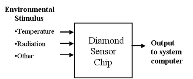
AET is developing diamond sensors that will be integrated into a silicon chip so that the information coming to the computer on-board the air vehicle can accurately process the data. To achieve this we are developing a system concept as illustrated in Figure 1. As seen here, the stimulus for the Diamond Sensor Chip can be any information from the environment including temperature, radiation, pressure, etc. Actually, this includes anything that can be detected by a sensor on-board Diamond Sensor Chip. The output of the Diamond Sensor Chip is a digital signal that goes to the aircraft computer. To implement this Nanoscale Sensor System, we propose the circuit concept shown in Figure 2. The temperature and radiation sensors will be a diamond resistive element that will be integrated with the monolithic silicon integrated circuit that makes up the primary part of the Nanoscale Sensor Chip. Researchers at Vanderbilt University will fabricate the diamond structures.
Fig 1 System Block Diagram
Fig 2 Diamond Sensor Chip Block Diagram
DIAMOND TECHNOLOGY
Diamond is generally recognized as a principal candidate for advanced semiconductor devices. The applications for diamond, more specifically in this case, CVD (chemical vapor deposited) diamond layers, include microelectronic devices, sensors, micromechanical systems, and high power structures. Major advantages for the use of diamond technology are its superior nuclear survivability and operation at much higher temperatures, high breakdown voltage, high electron saturation velocity, high carrier mobility, and large thermal conductivity.
Examination of the critical paths to useable advanced technology for SHM will invariably lead to the sensors at the edge of the networks. Certainly the network design is important – intelligent formulation will lead to faster/appropriate response and better SHM predictive behavior – but unless the data in is extensive, robust, fast and true, there is no real system monitoring.
The fundamental problem with existing sensor technology begins and ends with the sensor material Obviously, by virtue of precedent, silicon is the established sensor material, but because of its (relative) narrow band gap and the semiconductor physics approach to sensing, it is fundamentally limited by temperature, pressure, radiation exposure and most other variables of interest/stress to system health. In fact, silicon and related materials lose their useful sensing properties we// before many system health extremes (yellow/red zone range) are reached. This leads to either overdesign, dangerous extrapolative techniques, compromised remote sensor placement and/or undermonitored systems.
The need for sensors that will operate at significantly broader extremes (temp., radiation, etc.) and be economical and embedded (emplaced with no effect on system) is apparent and essential for next-generation systems. As discussed below,superior sensors will come from superior material and that material is diamond. First of all, diamond processing/deposition coating has become a commodity operation. It has become deployed routinely and "in production". This form of diamond is neither expensive nor exotic. Most importantly, it will extend the range_of sensing viability by many times as illustrated in Table I.
TABLE I. COMPARISON OF SILICON AND DIAMOND FOR SHM SENSOR PROPERTIES
|
Parameter |
Silicon Sensor Limits |
Diamond Sensor Limits |
|
Maximum Operating Temp. |
~ 150 C |
>500 C |
|
Minimum Operating Temp. |
~ -55 C |
< -270 C |
|
Junction Rectification |
-0.7V |
-0.1 V |
|
Pressure "Strength" |
1 |
>10X |
|
Radiation Tolerance |
-lMRad |
> 10 MRad |
|
Chemical Susceptibility |
Not Inert |
Inert |
As shown in Table I, silicon devices are more sensitive to temperature than are diamond devices. For example, as a thermistor, the thermal coefficient of resistance of diamond is well behaved [1].
TECHNOLOGY INTEGRATION
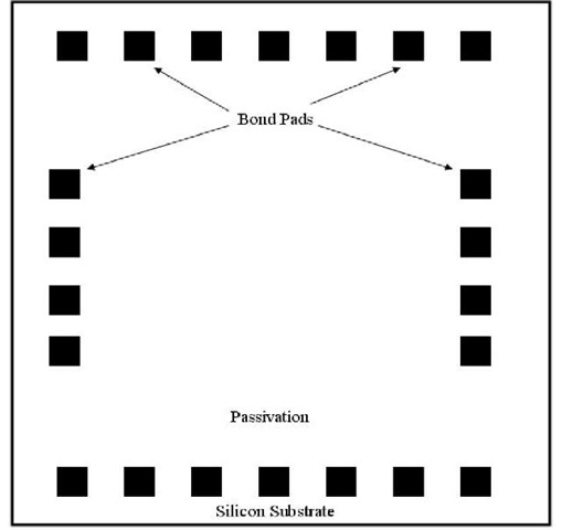
The researchers have developed a process flow for combining silicon integrated circuit structures and diamond sensors on the same chip. This flow utilizes all existing processes at Vanderbilt University and allows the use on a number of different silicon integrated circuit fabrication facilities. In addition, this flow is compatible with several different silicon technology types, including both standard CMOS and SOI-CMOS. The silicon process will proceed normally through circuit processing and nominally three metal layers and the passivation layer. The final step to be performed by the SOI foundry will be to open the bond pads in the passivation layer. This final topology is represented conceptually per a mask pattern for an IC chip as shown in Figure 3.
Fig 3 Die Topology After CMOS Processing
The wafers will then be transferred to Vanderbilt University for the processing steps to achieve diamond sensors. A 2-3 micron thick diamond film will be deposited at a temperature low enough to be compatible with the IC wafer (less than 450C). The diamond processing conformity will cover the topology typical of such CMOS wafers and will not require fine geometry photoresist.
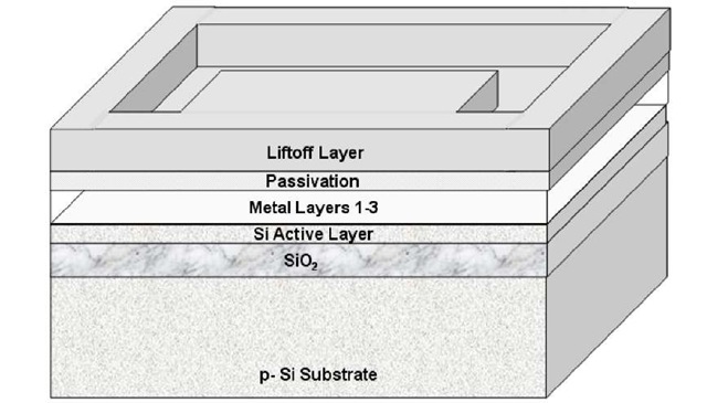
The first step performed in the creation of the diamond sensor is to deposit a lift-off layer comprised of Si02 ‘glass’ which may be applied by several techniques. The liftoff layer is then patterned and etched as shown in Figure 4.
Fig 4 Mask/Photoresist Define Lift-Off Layer
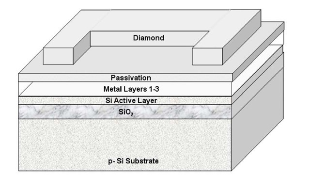
The diamond is then deposited at a low temperature (less than 450C). The optimum process to do this will be evaluated during the development phase, determining, for example whether the CVD or hot filament technique provides superior performance. The excess diamond is then ‘lifted off’ and the diamond sensor is delineated as shown in Figure 5. A liftoff procedure is presently preferred to achieve more benign conditions for the IC wafer substrate.
Fig 5 Lift-Off Excess Diamond
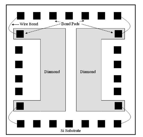
The metalization for contact to the diamond will be deposited and defined at Vanderbilt. The metal lies completely on the diamond, avoiding step coverage issues. We do not anticipate the need for a passivation layer over the diamond and metal layers at this time. Contact between the diamond sensor(s) and the SOI circuitry will be made with bond wires. The final topology is shown in Figure 6.
Fig 6 Die Topology after Diamond Contact Metal Deposition
CONCLUSIONS
AET and Vanderbilt University have developed an integrated circuit manufacturing process flow that combines both diamond and silicon technologies on a single IC chip. This chip will contain a variety of diamond sensors along with silicon CMOS readout circuitry. The application for the chip is to be embedded in the skin of air vehicles to improve the structural health monitoring of the system.
