The tailoring of strain distributions within semiconductor features represents a key method to enhance performance in current and future generations of complementary metal-oxide semiconductor (CMOS) devices. Although the impact of strain on carrier mobility in semiconductor materials was first investigated over 50 years ago [1,2], its implementation within the inversion layer of the channels in CMOS device channels has only occurred within the past decade. This includes the deposition of liner materials that possess significant values of residual stress [3]. Eigenstrained structures, deposited epitaxially within recesses on either side of the Si channel, can be used to induce either compressive strain in the channel region, by using materials that possess a larger lattice parameter than Si (e.g., SiGe)[4], or tensile strain, by using materials with a smaller lattice parameter (e.g., SiC). Because these methods generate heterogeneous strain distributions within the composite structure, it is critical to experimentally determine the distribution of strain across the current-carrying paths of the device and the surrounding environment.
Real-space x-ray microdiffraction measurements represent the optimal method to perform direct, in-situ characterization of strain within crystalline materials at a submicron length scale [5,6]. The diffraction facilities at the 2ID-D beamline at Argonne National Laboratory’s Advanced Photon Source were used for the x-ray microdiffraction measurements [6] with a nominal beam size of approximately 0.25 ^m. Samples under investigation included both CMOS devices possessing embedded stressor materials and silicon-on-insulator (SOI) structures with overlying stressor features. The embedded stressor devices, fabricated from 55 nm thick SOI layers, contained Sii.xCx with a C content, x, of 1.1% in the source and drain regions, approximately 1.85 ^.m in length. Because C has a smaller lattice parameter than that of Si, the e-SiC structures possess in-plane tensile stress, which is transferred into the adjacent, 60 nm long SOI channel. To obtain a reference value for the unrelaxed SiC strain, square pads 200 ^m in length, also consisting of heteroepitaxially deposited SiC, were characterized. Another set of SOI structures was fabricated possessing overlying stressor features, where compressively stressed Si3N4 films of approximately 105 nm thickness were lithographically etched to produce a matrix of rectilinear features possessing lengths of 2048 ^m and widths ranging from 1 ^m to 2048 ^m.
X-ray microbeam measurements of the embedded stressor CMOS device revealed that the out-of-plane strains in the e-SiC were approximately -0.355% within the vicinity of the SOI channel and -0.350% 0.8 ^m away from the channel [7]. Diffraction from the thin SOI layer underneath the e-SiC features indicated a small, tensile out-of-plane strain of 74 x 10-6. The difference between the two SOI diffraction peaks measured away from and at the channel contains the depth-averaged strain information from the SOI channel, corresponding to an out-of-plane compressive strain of -0.167%. The predicted out-of-plane strains for the e-SiC feature and SOI channel are -0.355% and -0.176%, respectively, as calculated using an Eshelby inclusion model [8]. The measured strain in the e-SiC regions match well, and the out-of-plane SOI channel strain is approximately 95% of the predicted value.
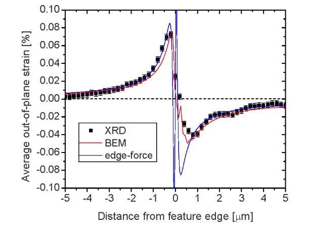
A mapping of the out-of-plane SOI strain distribution under the edge of a 2048 x 2048 ^.m Si3N4 feature edge is depicted in Figure 1. Simulated out-of-strain profiles using an anisotropic, edge-force model [9] and an elastically isotropic boundary element method (BEM) model [10] are included for comparison. The BEM calculated values capture the asymmetry exhibited in the strain distribution across the Si3N4 feature edge location and confirm a compressive blanket film stress of -2.5 GPa in the Si3N4. For the edge-force model, the predicted values diverge from the measured strain in the SOI underneath the Si3N4 feature within 1 ^m from the feature edge, or approximately 10 times the Si3N4 feature thickness, because peel and shear stresses at the Si3N4 / SOI interface cannot be captured by the edge-force model. Both experimental results and modeling clearly illustrate the extent to which strain fields can be generated in the vicinity of a free edge in a stressor material.
FIG. 1: Comparison of the experimentally measured and BEM calculated depth-averaged strain distribution in the SOI across the edge of an overlying 2048 x 2048 m Si3N4 feature.
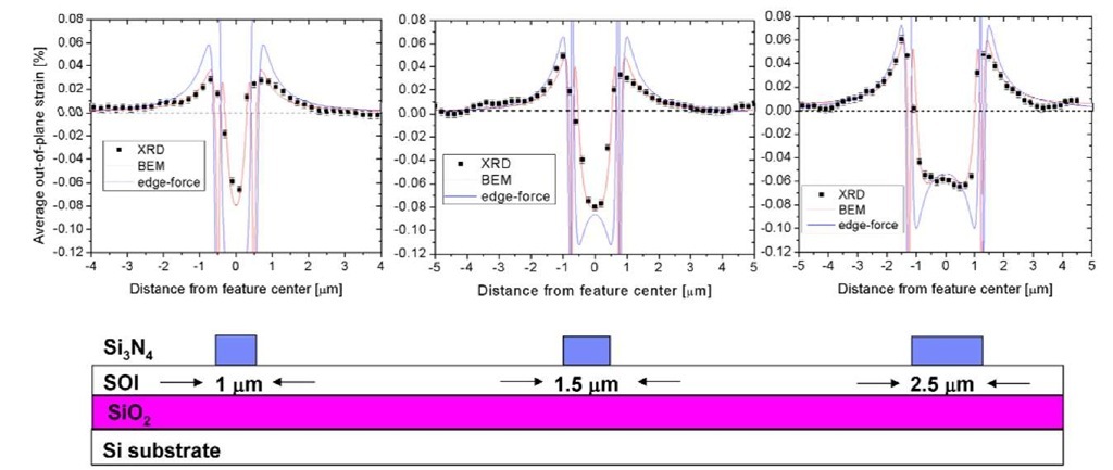
Figure 2 contains the measured and calculated out-of-plane SOI strain distributions under 1 ^.m, 1.5 ^m and 2.5 ^m wide Si3N4 features, respectively. There is a close correspondence between the BEM calculated values and the measured strain distributions outside of the immediate vicinity of the feature edges. In contrast, edge-force simulations exhibit a poor match to the measured strain values in the SOI underneath the stressor structures. The overlapping of strain fields induced by the feature edges dictates both the maxima in the depth-averaged strain observed in the SOI outside of the Si3N4 features as well as the shape of the distribution underneath the stressors.
FIG. 2: Comparison of the experimentally measured and calculated SOI strain distributions across 2048 x 1 ^m, 1.5 ^m and 2.5 ^m wide Si3N4 features.


