Band Structures for Some Metals and Semiconductors
Those readers who have skipped Sections 5.3 through 5.6 need to familiarize themselves with the (three-dimensional) first Brillouin zone for the face centered cubic (fcc) crystal structure (Fig. 5.19). The [100], the [110], and the [111] directions in k-space are indicated by the letters G — X, G — K, and r — L, respectively. Other directions in k-space are likewise seen. These specific symmetry points and directions are selected by convention from a much larger number of possible directions. They sufficiently characterize the properties of materials, as we will see below.
We inspect now some calculated energy-band structures. They should resemble the one shown in Fig. 5.4. In the present case, however, they are depicted for more than one direction in k-space. Additionally, they are displayed in the positive k-direction only, similarly as in Fig. 5.6 or 5.20.
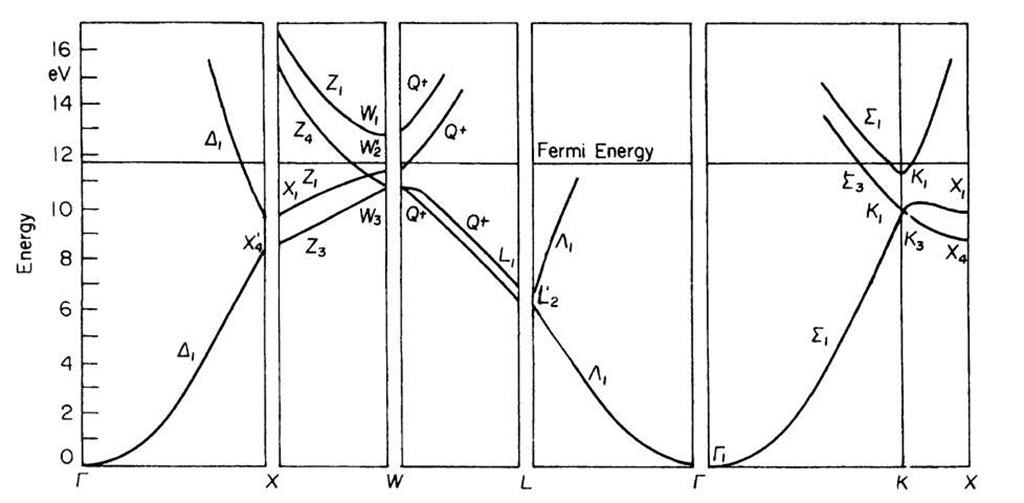
We start with the band diagram for aluminum, Fig. 5.21. We recognize immediately the characteristic parabola-shaped bands in the kx(G — X) direction as seen before in Fig. 5.4. Similar parabolic bands can be detected in the G — K and the G — L directions. The band diagram for aluminum looks quite similar to the free electron bands shown in Fig. 5.20. This suggests that the electrons in aluminum behave essentially free-electronlike (which is indeed the case).
We also detect in Fig. 5.21 some band gaps, for example, between the X4 and X1 symmetry points, or between W3 and W2. Note, however, that the individual energy bands overlap in different directions in k-space, so that as a whole no band gap exists. (This is in marked difference to the band diagram of a semiconductor, as we shall see in a moment.) The lower,parabola-shaped bands are associated with the aluminum 3s electrons (see topic 3).
Figure 5.21. Energy bands for aluminum.
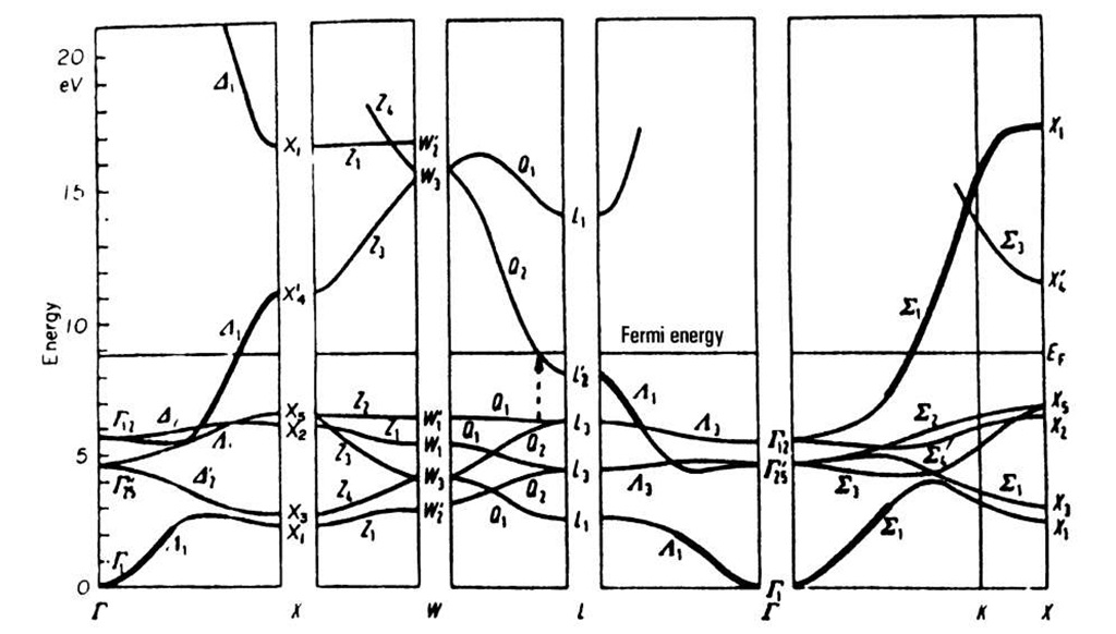
Figure 5.22. Band structure of copper (fcc).
These bands are therefore called "3s bands". The origin of the energy scale is positioned for convenience in the lower end of this s-band.
Next, we discuss the band structure for copper, Fig. 5.22. We notice in the lower half of this diagram closely spaced and flat running bands. Calculations show that these can be attributed to the 3d-bands of copper (see topic 3). They superimpose the 4s-bands (which are heavily marked in Fig. 5.22). The band which starts at T is, at first, s-electronlike, and becomes d-electronlike while approaching point X. The first half of this band is continued at higher energies. It is likewise heavily marked. It can be seen, therefore, that the d-bands overlap the s-bands. Again, as for aluminum, no band gap exists if one takes all directions in k-space into consideration.
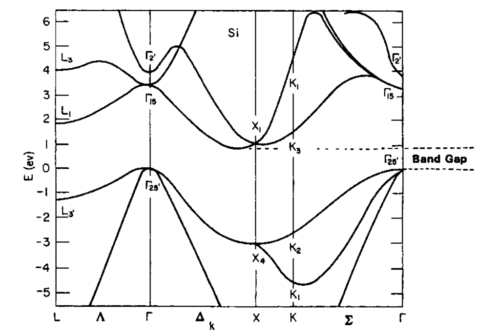
As a third example, the band structure of silicon is shown (Fig. 5.23). Of particular interest is the area between 0 and approximately 1 eV in which no energy bands are shown. This "energy gap," which is responsible for the well-known semiconductor properties, will be the subject of detailed discussion in a later topic. For semiconductors, the zero point of the energy scale is placed at the bottom of this energy gap, even though other conventions are possible and in use.
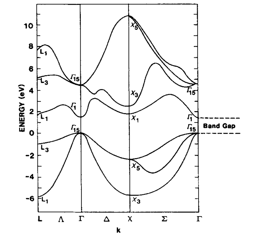
Finally, the band structure of gallium arsenide is shown in Fig. 5.24. The so-called III-V semiconductor compounds, such as GaAs, are of great technical importance for optoelectronic devices, as we will discuss in later sections. They have essentially the same crystal structure and the same total number of valence electrons as the element silicon. Again, a band gap is clearly seen.
Figure 5.23. Calculated energy band structure of silicon (diamond-cubic crystal structure).
Figure 5.24. Calculated energy band structure of GaAs.
It should be mentioned, in closing, that the band structures of actual solids, as shown in Figs. 5.21-5.24, are the result of extensive, computer-aided calculations, and that various investigators using different starting potentials arrive at slightly different band structures. Experimental investigations, such as measurements of the frequency dependence of the optical properties, can help determine which of the various calculated band structures are closest to reality.
Curves and Planes of Equal Energy
We conclude this topic by discussing another interesting aspect of the energy versus wave vector relationship.
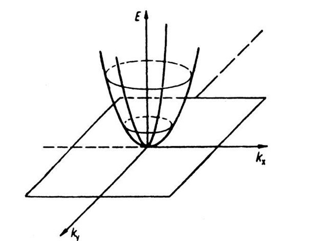
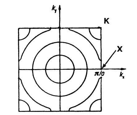
In one-dimensional k-"space" there is only one (positive) k-value which is connected with a given energy (see Fig. 5.1). In the two-dimensional case, i.e., when we plot the electron energy over a kx — ky plane, more than one k-value can be assigned to a given energy. This leads to curves of equal energy, as shown in Fig. 5.25. For a two-dimensional square lattice and for small electron energies, the curves of equal energy are circles. However, if the energy of the electrons is approaching the energy of the boundary of a Brillouin zone, then a deviation from the circular form is known to occur. This is shown in Fig. 5.26, where curves of equal energy for a two-dimensional square lattice are inserted into the first Brillouin zone. It is of particular interest that the energy which belongs to point K in Fig. 5.26 is larger than the energy which belongs to point X (see (5.8a) and (5.9a)).
Figure 5.25. Electron energy E versus wave vector k (two-dimensional). This figure demonstrates various curves of equal energy for free electrons.
Figure 5.26. Curves of equal energy inserted into the first Brillouin zone for a two-dimensional square lattice.
Consequently, the curves of equal energy for the first Brillouin zone may extend into the second zone. This leads to an overlapping of energy bands as schematically shown in Fig. 5.9, and in the band structures of Figs. 5.21-5.24. For copper and aluminum the band overlapping leads to quasi-continuous allowed energies (in different directions of k-space). For semiconductors the band overlapping is not complete, which results in the already-mentioned energy gap (Figs. 5.23 and 5.24).
In three-dimensional k-space one obtains surfaces of equal energy. For the free electron case and for a cubic lattice they are spheres. For a nonparabolic E-(k) behavior these surfaces become more involved. This is demonstrated in Fig. 5.27 for a special case.
Figure 5.27. A particular surface of equal energy (Fermi surface, see Section 6.1) and the first Brillouin zone for copper.
