Elements With Curved Surfaces
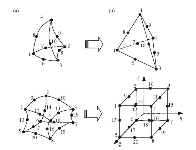
Using high order elements, elements with curved surfaces can be used in the modelling. Two relatively frequently used higher order elements of curved edges are shown in Figure 9.18(a). In formulating these types of elements, the same mapping technique used for the linear hexadron elements (Section 9.3) can be used. In the physical coordinate system, elements with curved edges are first formed in the problem domain as shown in Figure 9.18(a). These elements are then mapped into the natural coordinate system using Eq. (9.34). The elements mapped in the natural coordinate system will have straight edges, as shown in Figure 9.18(b).
Figure 9.18. 3D solid elements with curved surfaces. (a) Elements with curved surfaces in the physical coordinate system; (b) brick elements obtained by mapping.
Higher order elements of curved surfaces are often used for modelling curved boundaries. Note that elements with excessively curved edges may cause problems in the numerical integration. Therefore, more elements should be used where the curvature of the boundary is large. In addition, it is recommended that in the internal portion of the domain, an element with straight edges should be used whenever possible.
Case Study: Stress and Strain Analysis of a Quantum Dot Heretostructure
Quantum dots are clusters of atoms nanometres in size, usually made from semiconducting materials like silicon, cadmium selenide or gallium arsenide. What makes quantum dots interesting is that they have unusual electrical and optical properties, hence they have the potential for use in a wide variety of novel electronic devices, including light emitting diodes, photovoltaic cells, and quantum semiconductor lasers. An interesting way of fabricating such quantum dot structures is to actually grow the dots directly by depositing a thin film layer of material on a substrate under appropriate growth conditions. Usually, the thin film layer is of a different material to the substrate material, and thus such structures are also generally known as heterostructures. This growth mode is due to the mismatch in the lattice parameters of the different materials, and is known as the Stranski-Krastanow (SK) growth mode.
Figure 9.19. Schematic representation of a quantum dot heterostructure.
Study of such quantum dot heterostructures is actually a very active research area at the time at which this topic was written. In this case study, an example of modelling a 3D finite element model to analyse the stress distribution in and around such structures will be shown. The stress distribution actually affects the electrical and optical properties of the quantum dot structure. Furthermore, the quantum dot formation in multiple thin film layers is also very much dependent on this stress distribution.
Figure 9.19 shows a schematic representation of a quantum dot grown on top of the substrate and embedded in a cap layer. This is just a single quantum dot, and can probably be considered as a single basic unit of the heterostructure. In reality, there could be many of such quantum dots distributed on top of a layer of substrate. It can also be seen from the figure that the quantum dot is usually pyramidical or trapezoidal in shape. The pyramidal shape of the quantum dot is often approximated by using a 2D axisymmetric model of a cone by many analysts. However, it should be noted that using a 2D axisymmetric model is not fully representative of the pyramidal shape, and for the purpose of this topic, this case study will be using the 3D solid element to model the structure.
Modelling Meshing
As mentioned, the modelling of any 3D structure is generally more complex and tedious. In this case, eight-nodal, hexahedron elements are being used for meshing of the 3D geometry. It can be seen from Figure 9.19 that the problem domain is very much symmetrical.
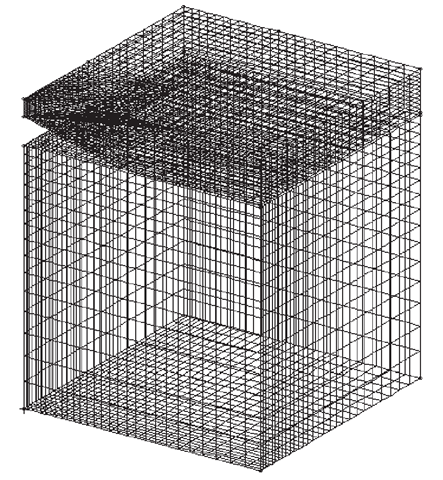
Figure 9.20. 3D mesh of the matrix.
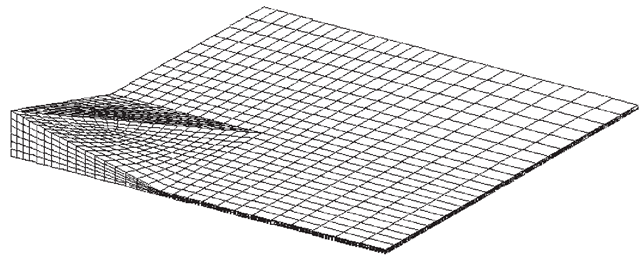
Figure 9.21. 3D mesh of the island.
Therefore, to work on a more manageable problem, a quarter of the model is being modelled using mirror symmetry. Note that it is also possible to use a one-eighth model, which then requires the use of Multi-Point Constraints (MPC) equations.
Proper meshing in this case is very important, as it has been found that a poor mesh usually yields bad results. The 3D mesh of the heterostructure is shown in Figures 9.20 and 9.21. The model is generally divided into two main parts geometrically for the analysts to distinguish them more conveniently. The parts of the heterostructure comprising the substrate and the cap layer, as shown in Figure 9.19, is grouped together as the matrix; and the parts of the heterostructure comprising the wetting layer and the quantum dot itself are grouped together as the island.
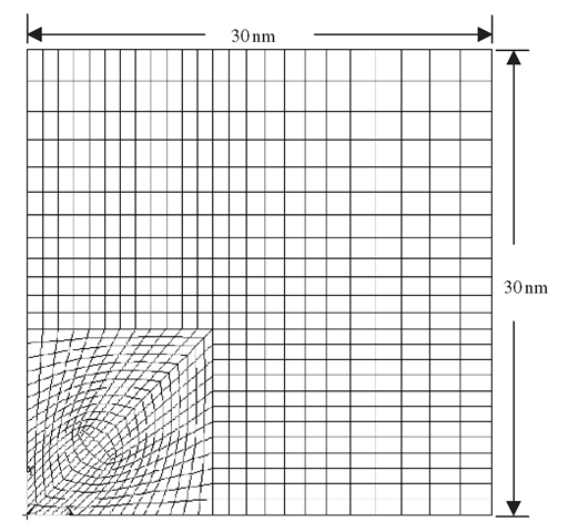
Figure 9.22. Plan view of finite element mesh of quantum dot heterostructure.
Table 9.1. Material properties of GaAs and InAs
|
Material |
E (Gpa) |
υ |
|
GaAs |
86.96 |
0.31 |
|
InAs |
51.42 |
0.35 |
Figure 9.22 also shows a plan view of the mesh of the island (or matrix). It can be seen how smaller elements are concentrated at and around the pyramidal quantum dot. To generate the mesh here, the analyst has employed the aid of automatic mesh generators that can still mesh the relatively complex shape of the pyramid with hexahedron elements. Some mesh generators may not be able to achieve this, and one may end up with either tetrahedron elements or a mixture of both hexahedron and tetrahedron elements.
Material properties
In this case study, the heterostructure system of Indium Arsenide (InAs) quantum dots embedded in a Gallium Arsenide (GaAs) substrate and cap layer is analysed. Therefore, the matrix part of the model will be of the material GaAs and the island part of the model will be of the material InAs. This is an example of the convenience of dividing the model into these two parts. It is assumed here that the materials have isotropic properties, listed in Table 9.1.
Constraints and boundary conditions
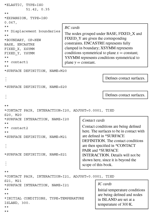
As the model is a symmetric quarter model, symmetrical boundary conditions must be applied. Here it means that the nodes on the planes corresponding to x = 0 nm, y = 0 nm, x = 30 nm and y = 30 nm have their displacement components normal to their respective planes constrained. Another displacement boundary condition would be the base of the matrix, where all the displacement components of the nodes are constrained.
There is also a contact constraint condition imposed between the outer surfaces of the island and the surfaces of the cap layer and the substrate in the matrix. Contact modelling is a relatively advanced technique, and will not be covered in this topic. Basically, contact modelling is used to model the sliding or the movement between two surfaces. ABAQUS offers a ‘tied’ contact condition where the two surfaces in contact are actually tied to one another. This ‘tied’ contact condition is used here to model the bonding between the island (InAs) and the matrix (GaAs).
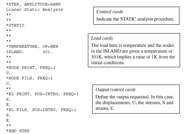
There is actually no load acting on this model. Rather, thermal expansivity is being made use of to simulate the strain induced due to the lattice mismatch between GaAs and InAs. The strain induced due to the lattice mismatch can be calculated from the lattice parameters to be -0.067. To represent this lattice mismatch, a corresponding thermal expansion coefficient of aT = 0.067 is applied to the elements in the island, and the temperature is raised by 1 K. This would effectively result in an expansion of the island, and because it is constrained by the matrix, thermal strain corresponding to the lattice mismatch strain is induced. Note that this thermal expansion does not take place in the physical case, but is just used to produce the mismatch strain. This thermal strain actually contributes to the force vector in the finite element equations.
ABAQUS Input File
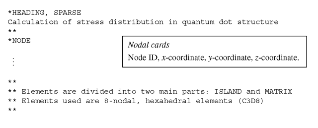
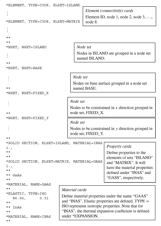
Part of the ABAQUS input file for the problem defined above is shown below. As the problem is quite large, the full input file would consist of a large amount of data defining the nodes, elements, and so on. As such, the full data will not be included here and some parts of the input file that have been explained in previous case studies will not be explained again here.
The input file provides the information ABAQUS needs to perform tasks like forming the stiffness matrix and the force vector (no mass matrix, since this is a static analysis). The full input file may consist of many pages, which is common for large problems.
Solution Process
The information provided in the input file is very similar to previous case studies in this topic. The nodal and element connectivity information is read for the formulation of the element matrices. The element type used here is C3D8, which represents a 3D, hexahedral element with eight nodes. More 3D element types are also available in the ABAQUS element library. The material properties provided in the input file will also be used to formulate the element stiffness matrix (Eq. (9.51)). Recall that the integration in the stiffness matrix is usually carried out using the Gauss integration scheme sampled in three directions, and in ABAQUS, the default number of integration points per face of the hexahedral element is four, making the total number of integration points per element 24. All the element matrices will be assembled together using the connectivity information provided. Application of the boundary conditions and the thermal strain induced by the thermal expansion is carried out by the specifications in the boundary cards and the load card. Finally, the finite element equation will be solved using the algorithm for static analysis.
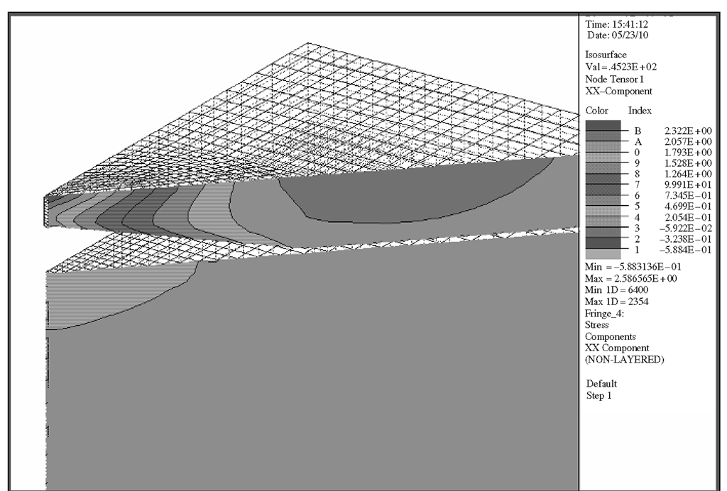
Figure 9.23. Stress, σχχ distribution of plane θ = 45° in matrix.
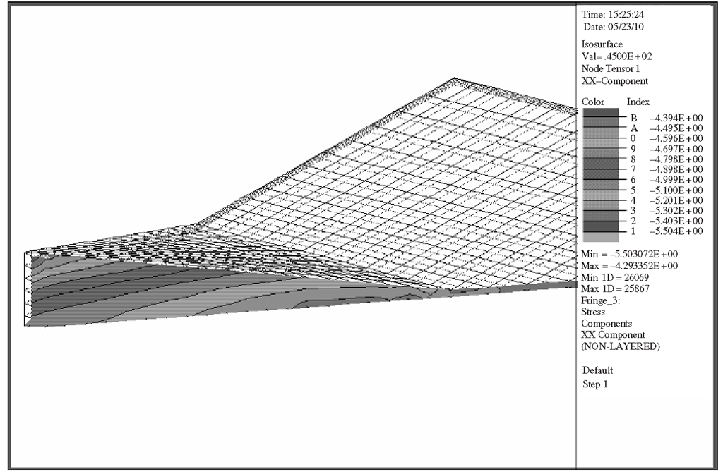
Figure 9.24. Stress, σχχ, distribution of plane θ = 45° in island.
Result and Discussion
Running the problem in ABAQUS, we are able to get the stress distribution and the strain distribution as requested in the input file. Figures 9.23 and 9.24 show the stress distribution obtained in the matrix and island, respectively, of a particular plane of θ = 45°, where θ is measured from the x-z plane counter-clockwise. Despite the extra effort in the meshing of a 3D model, the advantage is that it enables the analyst to view, in this case, the stress distribution in any arbitrary plane in the entire model. This would be difficult to achieve if a 2D, axis-symmetric approximation is carried out instead. From the stress distribution, one can observe that there are compressive stresses in the island and tensile stresses in the matrix area above the island. In the island, there is also stress relaxation in the quantum dot, with the maximum stress relaxation at the tip of the pyramidal quantum dot. This actually verifies the thermodynamics aspect of quantum dot formation, since the formation of a quantum dot results in a lower energy level (lower elastic strain energy). The tensile stress in the matrix area above the quantum dot is also important, as this stress actually causes a subsequent quantum dot to be formed directly above the buried quantum dot when a subsequent InAs layer is deposited.
