Several mid- and high-range PIC devices feature a small EEPROM scratchpad memory that can be controlled and accessed indirectly via Special-Purpose Registers (SPRs) in the same manner as other peripheral devices. An integral non-volatile scratchpad enables the programmer to read and modify static data, such as the odometer tally in a car, which needs to be retained in the absence of a power supply – see Example 12.3. Although this facility can be implemented using an external EEPROM memory, such as the 24LC01 of Fig. 12.22,where only a modest amount of non-volatile data needs to be stored, integral EEPROM storage increases reliability and reduces cost, size and power requirements.
Our objective here is to examine the non-volatile storage facilities available to members of the mid-range PIC family. After reading this topic you will:
• Be familiar with the characteristics of the EEPROM Data memory.
• Know how to both read and write data to the EEPROM module.
• Understand how the main flash EEPROM Program memory can be used in some devices to store and retrieve non-volatile data.
• Be able to contrast the EEPROM Data module and flash Program memory as a location for non-volatile data.
The PIC16C83/4 introduced in 1994, was the first PIC device to use EEPROM technology for its main Program store. As we gave seen in Fig. 2.12, Electrically Erasable PROM is similar to EPROM but does not require UV radiation to erase data. Although EEPROM technology is more expensive than EPROM, its use in implementing the Program store is convenient in prototyping and educational/hobbyist applications. Along with this innovation, an EEPROM peripheral module was featured which enabled the programmer to store up to 64 bytes of nonvolatile data independently of the normal file register memory.
The PIC16C83/4 and its analogous flash EEPROM memory successor, the PIC16F83/4, remained the only EEPROM family member until the introduction of the PIC16F87X in 1998. As of 2000, Microchip were committed to introduce flash EEPROM versions of most of their standard mid-and high-range devices. Thus, for example, the PIC16F74 will shadow the PIC16C74 processor.
In this topic we will use the 18-pin PIC16F83/4, 28-pin PIC16F873/6 and 40-pin PIC16F874/7, here denoted the PIC16C8X and PIC16F87X lines respectively, as our exemplar. However, before examining the details, it is instructive to look at an application requiring the use of non-volatile storage. A good example of this is the smart card of Fig. 12.1.Here we need to store, amongst others, the card account number, PIN number, start and expiry dates. Some of this data, such as the account number, is essentially fixed. Security data may need to be altered occasionally by the user from a terminal. If the card is used as a cash card its credit will need to be charged via an ATM and discharged when payments are made. The size and cost sensitivities of a smart card processor is such that integral EEPROM data storage is highly advantageous.
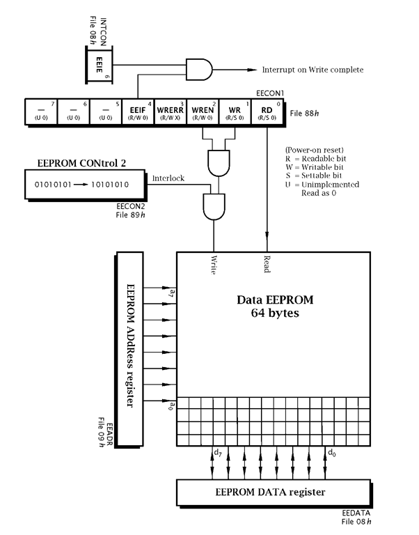
Figure 15.1 shows the logic organization of the PIC16F8X EEPROM Data module.6 The memory matrix is not part of the normal Data and Program stores but is indirectly accessed via four SPRs which address the target byte, collect/hold data and control the read and write processes.
EEPROM matrix
The mid-range EEPROM Data module architecture supports 256 byte cells. The bottom 64 locations are implemented in both the PIC16F83 and PIC16F84 devices. The PIC16F873/4 has a capacity of 128 bytes and the PIC16F876/7 implement all 256 memory cells. Key features are:
• 1,000,000 minimum (107 typical) Erase/Write cycle endurance for each cell.
• Maximum Erase/Write cycle time 8 ms.
• Data retention greater than 40 years.
The EEADR register located at File09h can address up to a maximum of 256 bytes of EEPROM data. Where less than maximum capacity is implemented, unused upper address bits must be 0 to ensure that the address is within the physical address space. In the PIC16F8X allowable addresses are in the range 00-3Fh.
The EEDATA register located at File 08h either holds the 8-bit datum read out of the addressed cell or the byte the programmer wishes to write to the target EEPROM cell.
EEPROM Control register 1 EECON1
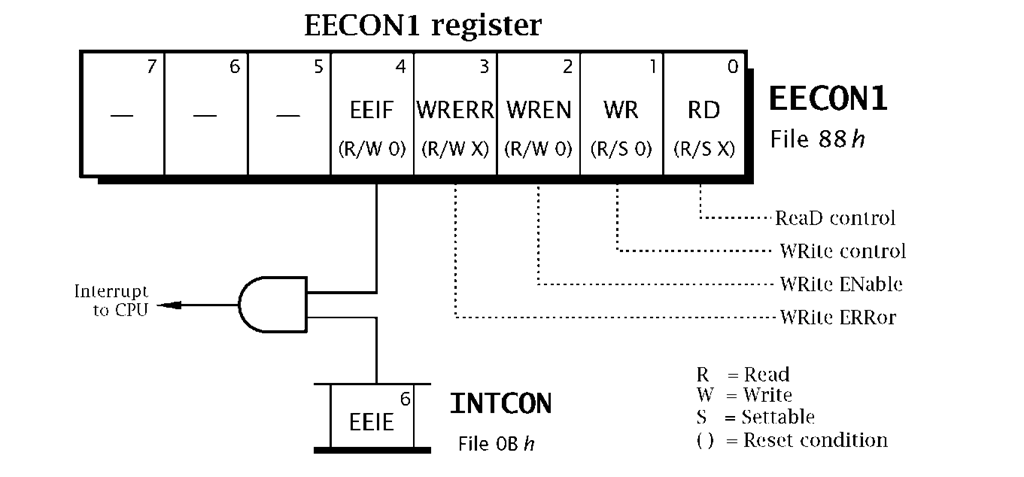
The EEPROM module has two modes of operation, with EECON1 located at File 88h in Bank 1 controlling and monitoring the Read and Write cycles – see Fig. 15.2.
Fig. 15.1 The PIC16F8X Data EEPROM module.
Fig. 15.2 The PIC16F8X EECON1 register. EEPROM Control register 2 EECON2
This register located at File 89h is not physically implemented – it always reads as zero. Rather the action of writing the successive code pattern 01010101 — 10101010 with no interruption is used to unlock the Write cycle. This arcane incantation is deliberately designed to convolute the process as security against unintended alterations in the data.
In order to read a specified datum from the EEPROM module we have to implement software to execute the task list:
1. Copy the target cell’s address to EEADR.
2. Set RD to 1 to initiate the Read cycle.
3. RD is automatically cleared immediately and the target 8-bit datum can be read from EEDATA any time from the next instruction cycle as convenient.
Program 15.1 Retrieving a byte from the EEPROM Data module.
Subroutine EE_GET in Program 15.1 directly implements this process and illustrates the return of the datum from the EEPROM cell to the Working register. The datum will remain in EEDATA until the register is reused.
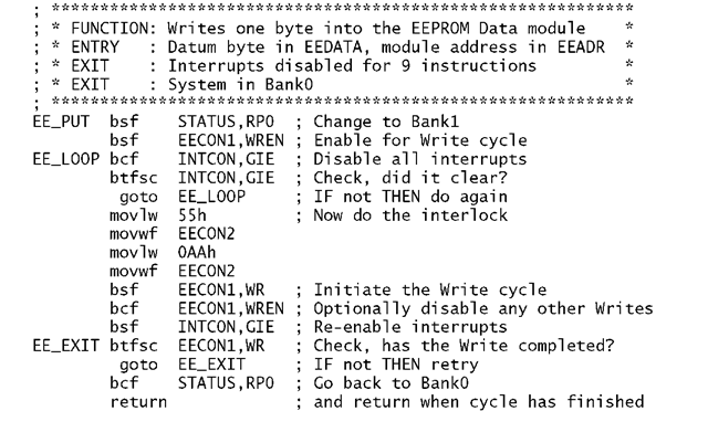
Writing data to the EEPROM Data module is deliberately made more Byzantine to reduce the chance of a spurious Write corrupting the data due to a software bug or processor malfunction because of, say, a power glitch. The task list to write a datum to a specified cell is:
1. Copy the target cell address to EEADR.
2. Set WREN in EECON1[2] to enable the Write process.
3. Disable all interrupts.
4. Send 55hto EECON2.
5. Send AAhto EECON2.
6. Set WR to initiate the Write cycle.
7. Clear WREN.
8. Enable interrupts.
9. Wait until WR returns to zero, signalling the completion of the Write cycle, and exit.
The Write cycle will not initiate if the interlock sequence items 4 – 6 is not exactly followed without interference. For example; in an interrupt-driven system an interruption during the interlock sequence will abort the Write cycle. Thus in this situation interrupts should be disabled by clearing GIE until the Write cycle has been initiated, otherwise this step can be omitted.
If desired the completion of the Write cycle can be used to interrupt the processor. This is enabled by setting the EEIE mask bit in INTCON[6]. When the interrupt flag EEIF, located in EECON1[4], is set in the normal way then the interrupt is generated. It should be cleared in the ISR.
It is possible that the processor is reset, for example by a Watchdog overflow, before the Write cycle is complete. In this situation, the EEPROM datum may be corrupt. The WRERR flag in EECON1[3] will be set if the Write operation has been prematurely terminated with a Reset action. If this is not the case, when the cycle is complete the datum may be read back and verified to give extra security. The WREN bit may be cleared at this point to help prevent an accidental Write. Doing this before the Write is complete will not affect the operation.
Program 15.2 implements this task list. Both EEDATA and EEADR are set up by the caller program with the byte data and address. The subroutine is not pulled out until the Write cycle has completed; typically 4 ms. This ensures that these SPRs will not be altered during the cycle which may possibly give an erroneous outcome.
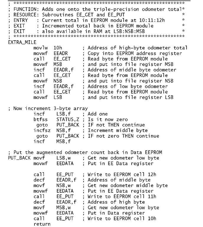
In order to illustrate these concepts we will repeat Example 12.3 replacing the external serial EEPROM with the internal module. We will assume that the odometer count is located at EEPROM cells 10 – 1 2h.
Program 15.2 Putting a byte into the EEPROM Data module.
The coding shown in Program 15.3 makes use of the two subroutines EE_GET and EE_PUT to read and subsequently write the three odometer bytes from the EEPROM Data module. The address of the first (highest) byte is copied into EEADR at the beginning of the subroutine and is subsequently incremented and decremented in situ to point to the appropriate datum.
Once the 3-byte odometer state has been fetched and copied into memory it is incremented in exactly the same manner as in Program 12.15.The augmented array is then written back into EEPROM in the opposite sense as it was read, with EEADR being decremented. The EE_PUT subroutine checks that the Write cycle has been completed before returning and thus timing need not be checked by the calling program.
As well as altering data under program control it is possible to initialize the state of the EEPROM Data module when the executable program is being externally blasted into the Program memory; as illustrated in Fig. 10.5(a).The area of Program memory beyond the user Program store belongs to the special test/configuration memory space 2000h- 30FFh and can be accessed only during external programming. In Fig. 10.5(b) we observed that the Configuration fuse word is located at 2007h. The EEPROM module also lies in this space located at 2100h-21FFh. For example, to store the value of sine every 10° between 0° and 90° as part of the program source code we have:
where the assembler directive de (Data EEPROM) specifies the comma delimited list of data. Once the PIC has been programmed, the contents of the EEPROM Data module will look like Fig. 15.3.
Program 15.3 Incrementing the non-volatile odometer count in Data EEPROM.
Fig. 15.3 The first 32 bytes of EEPROM holding the sine look-up table.
Any data programmed in the way can be subsequently read by the program. For example, to read sin(50) the contents of EEPROM module location 05h is read, giving from our diagram C4h or 196 decimal (|f§ = 0.76525).
Although such load-time data is non-volatile it can be altered from within the program at run time. The Code Protection fuse does not secure data in the EEPROM Data module from modification, only code in the true Program store is protected.
Although it is possible to initialize the Program store in a similar manner using the dw (Data Word) directive in a similar manner, as shown in Program 15.6, this is of little use as the Harvard architecture’s separation of Data and Program store memory spaces means that there is no way an instruction can access this data.7 However, newer 16-bit PIC devices with a Flash EEPROM Program store allow the program to read and write such data in a similar indirect manner to that used for the EEPROM Data module.
To illustrate these devices we will be using the PIC16F87X line. Like the PIC16F8X PICs, these devices all have a main Program store implemented using Flash EEPROM technology as well as a standard EEPROM Data module. Besides the EEPROM module they have the same range of integral peripheral devices described in previous topics, but slightly enhanced. For example, the Analog module has a 10-bit resolution and the Synchronous Serial port has hardware Master I2C modes.
To cope with the extra SPRs and Data memory the Data store is organized into four banks. Those relevant to EEPROM facilities are located in Banks 2 and 3 and so both RP0 and RP1 bits in the Status register need to used to change bank.
Four devices are represented in this line:
This 28-pin device has a 4 Kbyte flash Program store and 128-byte EEPROM Data store together with a 192-byte file register store. It is pin compatible with the PIC16C73 device.
This 40-pin device has a 8 Kbyte flash Program store and 256-byte EEP-ROM Data store together with 192 file registers. It is pin compatible with the PIC16C74 device. PIC16F876
This 28-pin device is the same as the PIC16F873 but with twice the Program store capacity at 8 Kbytes and double the EEPROM Data module capacity at 256 bytes The file register store is increased to 368 file registers.
This is a 40-pin version of the PIC16F876. Key EEPROM properties are:
• 100,000 minimum EEPROM Data module Erase/Write cycle endurance per cell.
• 1000 minimum flash EEPROM Program store Erase/Write cycle endurance.
• Maximum Write/Erase time 8 ms (typical 4 ms) for both the Data module and flash memory.
Of particular note is the endurance limit of 1000 Write cycles for the flash EEPROM. Whilst this is entirely satisfactory when changing the device’s program, it is a limitation for some non-volatile data storage situations. Thus flash Program memory storage is more applicable to constant data, such as the sine lookup table, rather than for information that requires frequent update, such as the odometer.
Flash EEPROM has a smaller geometry than normal EEPROM. Whilst this speeds up its operation, charges which eventually trap in the floating gate insulation have a disproportional effect on the storage mechanism and leads to earlier deterioration.
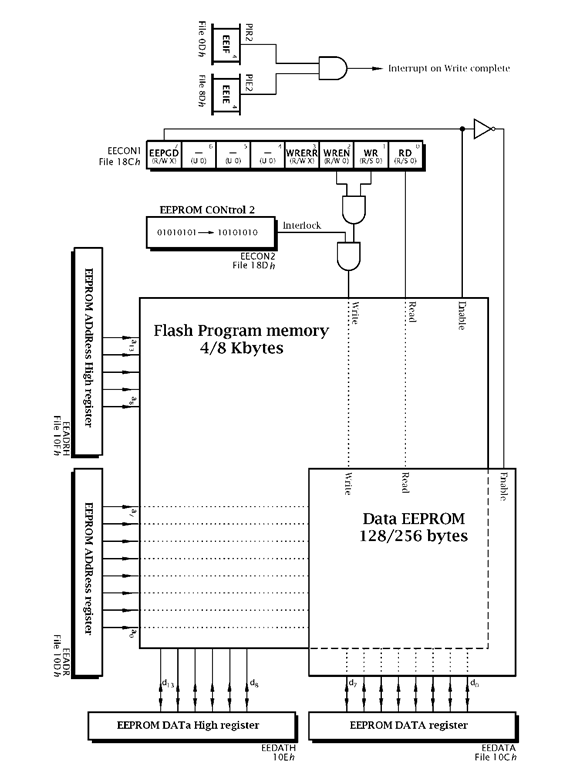
Figure 15.4 shows the PIC16F87X EEPROM Data module with the flash Program store superimposed. This form of representation is used as the EEDATA and EEADR registers are common to both EEPROM arrays. Of course, the flash Program store is larger both in the number of cells (8 Kbytes against 256 bytes) and in cell size (14 bits against 8 bits). Thus both Data and Address registers have the high-end extensions EEDATH and EEADRH respectively to cope with this additional capacity.
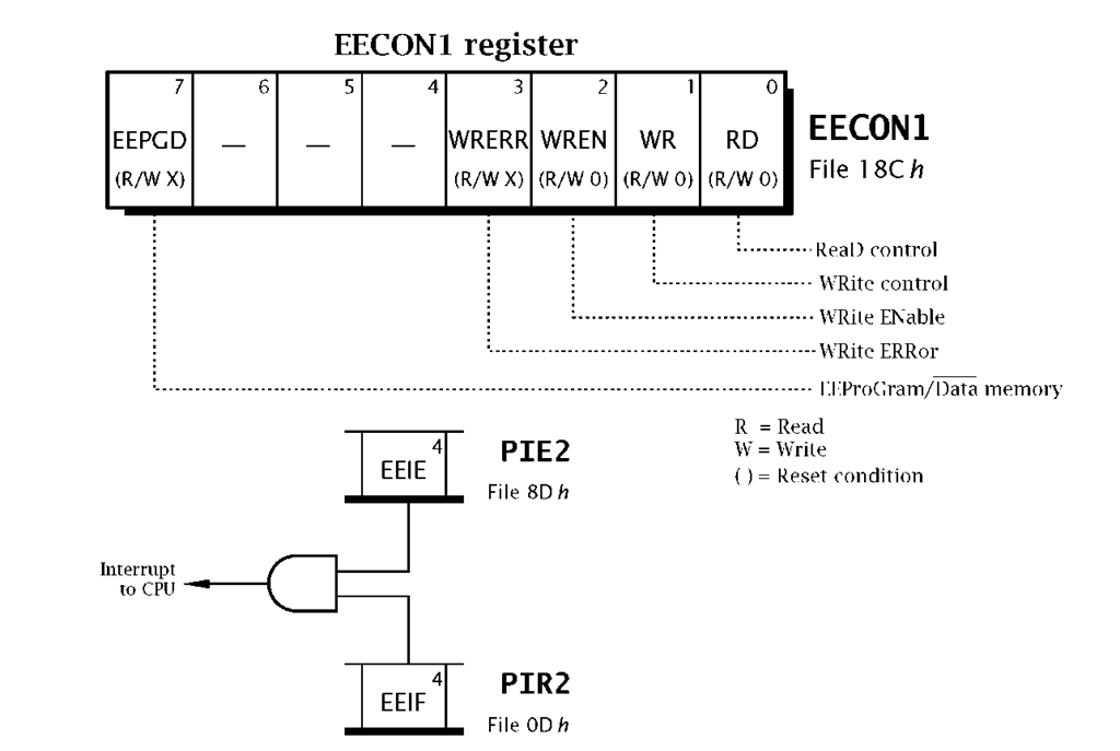
As we shall see, the process of reading from and writing to either array is similar. The target module is chosen using the EEPGD (EEProgram/Data) control bit control bit in EECON1[7]. Apart from this additional bit and the removal of the EEIF interrupt flag to the PIR2 register, the EECON1 register of Fig. 15.5 is identical to the basic PIC16F8X version shown in Fig. 15.2. The virtual EECON2 interlock register remains the same.
Fig. 15.4 The PIC16F87X flash and Data EEPROM storage system.
Fig. 15.5 The PIC16F87X EEPROM Control register 1.
Reading and writing to the EEPROM Data module is identical to that used for the more basic PIC16F8X device. The only change necessary to subroutines EE_GET and EE_PUT relates to the Bank 2 location of EEDATA and EEADR and Bank3 for EECON1 and EECON2.
