It is relatively easy to generate a PWM waveform solely in software by simply counting and setting a port pin when the count rolls over to zero and resetting the pin when it equals the datum representing the duty cycle. Thus if the duty cycle datum was 9Fh and the period count was module-256 (00-FFh) then the average power would be 62.5% (|).
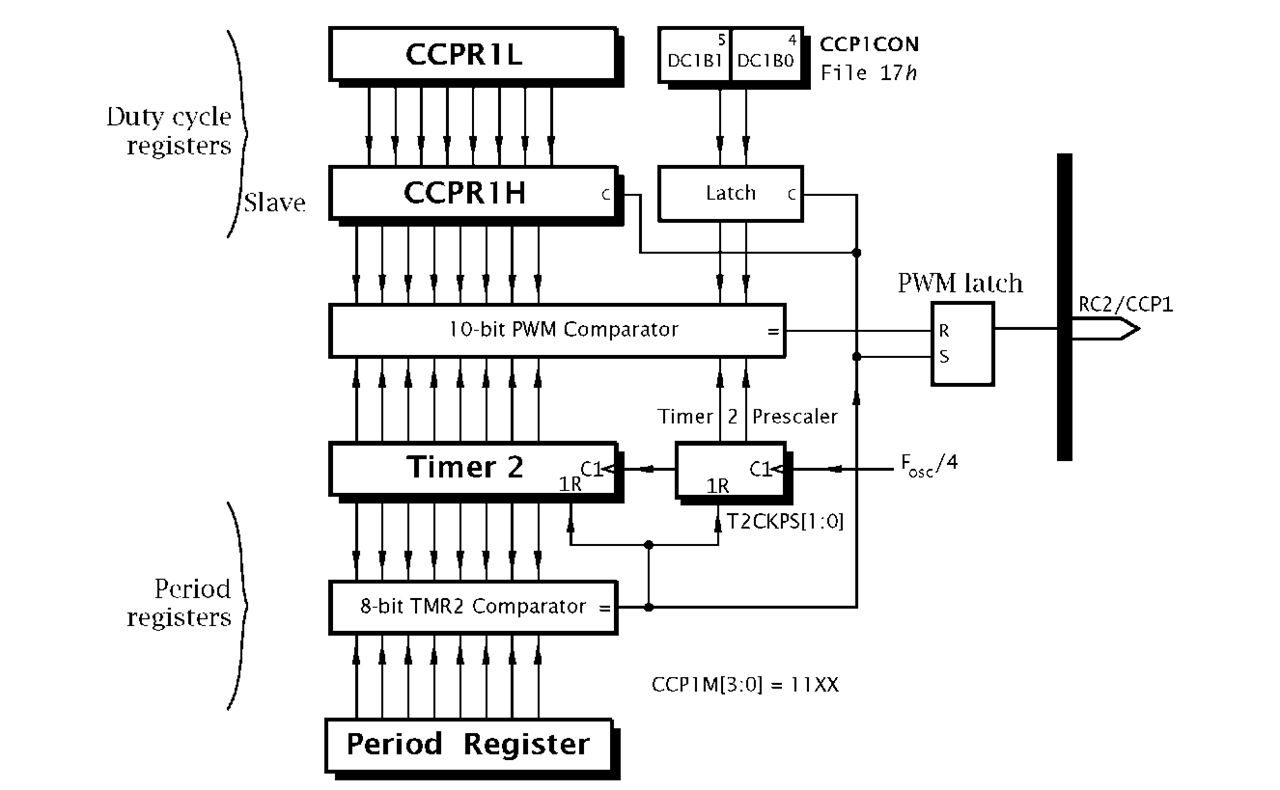
CCP modules have a PWM mode in conjunction with Timer 2, as shown in Fig. 13.10. Here Timer 2 runs with a period determined by the main crystal, prescaler and Period Register 2 as previously described. When the Timer 2 comparator causes the count to reset, it also sets the PWM latch. This gives the PWM repeat period.
A second CCP equality comparator matches the 10-bit duty cycle number which is set up by the program in CCPR1L and the two bits DC1B[1:0] (Duty Cycle 1 Bits) in CCP1CON[5:4]. Taken together this gives a 10-bit duty-cycle datum DC1B[9:0]. This datum is loaded into the CCPR1H and a slave 2-bit latch each time Timer 2 rolls over. CCPR1H is not directly writable to in this mode. Thus we have the following sequence of operations repeated indefinitely:
Fig. 13.10 Timer 2 and the PWM CCP mode.
1. Timer2 increments.
2. When Timer 2:Prescaler equals DC1B[9:0] the PWM latch resets and pin CCP1 goes low.
3. The next clock pulse after Timer2 reaches the datum in PR2 it is reset. The PWM latch is set, CCP1 goes high and the 10-bit slave duty cycle register/latch us updated.
4. Goto item 1.
From the above description we see that:
• The PWM period is set by the Timer 2/PR2 time-out.
• The duty cycle is set by the 10-bit datum in CCPR1L:CCP1CON[5:4].
• The duty cycle datum can be glitchlessly changed by the software at any time by updating the slave registers and will take effect in the PWM period following this update.
• The RC2/CCP1 pin direction should be set to output.
Where the Timer 2 prescale is set to 1:1 the lower two bits used on the timer side are the quadrature clock phases described in Fig. 4.4.This gives a period resolution equal to the crystal period. In all cases the datum in CCPR1L must be smaller than that in PR2, otherwise the PWM latch will never reset!
If PR2 is FFh then the resolution of the system is a full ten bits. Smaller values of Timer 2 period data will reduce this resolution. For example, if PR2 = 3Fh then the resolution is reduced to eight bits – six in PR2 and two in the prescaler.
For our example let us assume a crystal frequency of 20MHz, a prescale ratio of 1:16 and a PR2 value of FFh. In this case the PWM frequency is ^ x jg x 256 = 1.22 kHz. A prescale ratio of 1:1 would increase the period frequency to 19.53 kHz. Reducing the value in PR2 would also increase the repetition frequency. The programmer need only place the duty cycle datum in CCPR1L and CCP1CON[5:4] (the latter can be left at its reset value of zero if the datum is to be treated as 8-bit) and a PWM signal will automatically be generated with no software overhead. Set up code for this instance would be:
The Timer 2 postscaler does not affect the PWM generation but still sets the TMR2IF in the normal way. The CCP1IF is not altered in this mode.
If a second CCP module is used, an extra PWM output at pin RC1/CCP2 is available with a separate duty cycle but an identical period, as Timer 2 is a shared resource.
Examples
Example 13.1
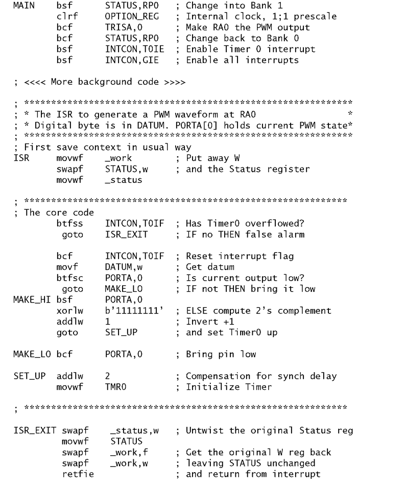
Show how you could use Timer 0 to generate a PWM version of a digital byte in file register DATUM using pin RA0 as the output. Assuming an 8 MHz crystal, calculate the PWM duration.
Solution
Timer 0 will give a time-out related to a number loaded into the timer at the beginning of the period. If we load in the the 2′s complement of the byte (the negative value) then the duration will be proportional to this value – the larger it is the longer the timer has to count before overflowing. Conversely loading in the value of DATUM will give a time-out duration inversely proportional to the value. By alternately loading the 2′s complement of DATUM and making the pin high followed by DATUM itself making the pin low will give us a total period approximately the same as a total Timer 0 time-out as if counting through all 256 states.
The coding of Program 13.5 sets up Timer 0 to count 2 MHz internal clock cycles with no prescale. Thus the total PWM rate is 256 or 7.8125 KHz. When Timer 0 overflows it generates an interrupt. The ISR checks the state of P0RTAA[0] and if 0 changes its state and then calculates the 2′s complement of the data byte (invert plus one). However, there is a 2-cycle delay in Timer 0 responding when its state is changed due to the clock synchronizer circuit and so another two is added to compensate for this extra delay. If the port pin was already 1 then it is zeroed and the datum itself plus the compensatory two is written into Timer 0.
Adding the compensation will cause problems at either extremes of the mark:space ratio. Why is this so and what action could you take to ameliorate it?
Example 13.2
A certain tachometer is to register engine speed in the range 0-12,000 rpm (revolutions per second). The engine generates one pulse per revolution and it is intended that a PIC16C74 be used to count the number of pulses each second and calculate the equivalent rpm. Using two of the three available timers can you design a suitable hardware-software configuration?
Solution
Program 13.5 Pulse-Width Modulation using Timer 0.
A speed of 12,000rpm translates to a maximum pulse count of 200rps (revolutions per second). Thus we propose to use Timer 0 as the pulse counter driven from pin T0CKI with no prescaler.
Timer 1 in conjunction with CCP1 set to a Compare mode will give a 1-second time-out if it uses its own oscillator and a 32.768 kHz watch crystal together with a count spanning 0000-7FFFh. However, to simplify the mathematical relationship rpm = rps x 60 it is proposed to shorten the timebase by the factor![]() to implement the equivalent relationship
to implement the equivalent relationship
![tmp9307_thumb[2][2] tmp9307_thumb[2][2]](http://what-when-how.com/wp-content/uploads/2011/06/tmp9307_thumb22_thumb.png) The final x64 can easily be implemented by either shifting left six times (>>6) or more efficiently placing the rps count as the high byte of the double-byte rpm datum and shifting right twice; i.e.:
The final x64 can easily be implemented by either shifting left six times (>>6) or more efficiently placing the rps count as the high byte of the double-byte rpm datum and shifting right twice; i.e.:
This is considerably more efficient that using a 1 second timebase and multiplying by 60.
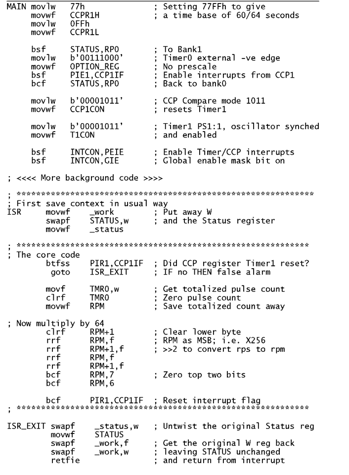
One possible solution is shown in Program 13.6. Here the initialization code implements the following task list:
• Set Timer 0 to count![]() events at T0CKI.
events at T0CKI.
• Set CCP1 to Compare mode 1011 to reset Timer 1 on equality.
• Enable an interrupt from this event.
• Set up the CCPR1H:L to set the timebase to![tmp9310_thumb[2][2] tmp9310_thumb[2][2]](http://what-when-how.com/wp-content/uploads/2011/06/tmp9310_thumb22_thumb.png) .
.
The ISR itself simply copies the rps reading from Timer 0, zeroing it and then converts the reading to rpm as described above. After the two shift right operation >>2, the top two bits of RPM are cleared to remove erroneous carry-ins. The resulting 14-bit datum in RPM:RPM+1 is the required outcome which can then perhaps be used by the background program to activate the display or maybe transmit the data to a computer over a serial link.
Example 13.3
A PIC16C74 is to be used to measure the duration of an event. This duration is the time a signal is high, as shown in Fig. 13.11. You an assume that the main crystal is 8 MHz and the duration of the event is guaranteed to be no more than 100 ms.
Solution
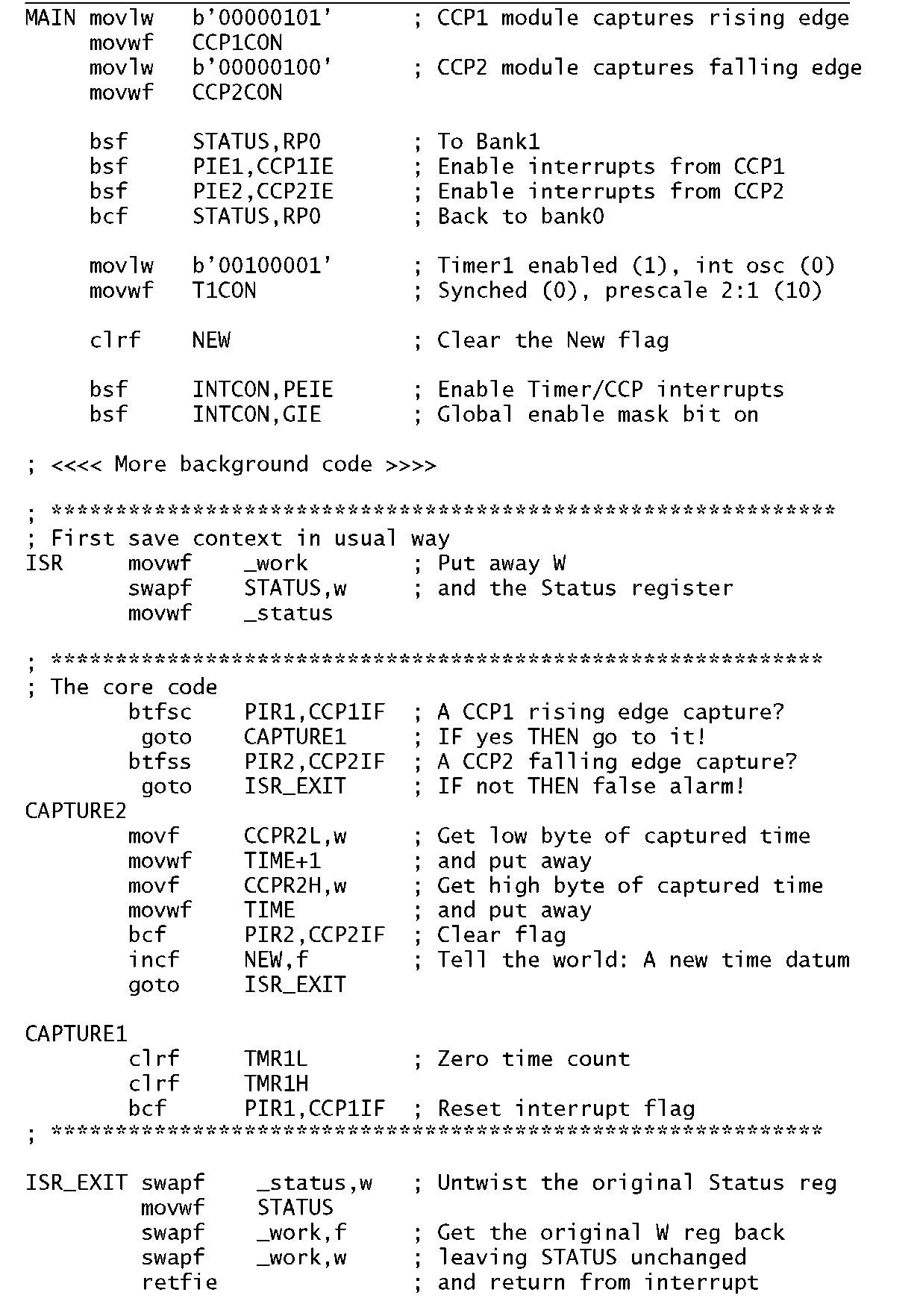
One way of tacking this problem is to feed the signal shown in the diagram into both pins RC1 and RC2 in parallel. Using one CCP module to capture the rising edge and the other to capture the falling edge gives the duration as the difference in the two captured values. In Program 13.7 Timer 1 is zeroed on a rising edge and thus the second captured Timer 1 state is our duration. If we use a prescale ratio of 1:4 and the internal clock then we have as our counting rate 500 kHz; i.e. the system resolution is 2 /is. The overall maximum duration that can be measured in this way is 216 x 2 = 131,077/s which is large enough not to overflow.
Program 13.6 Tachometer software.
1 Number representation. – Hexadecimal: Denoted by a following h, eg. 41h, or a leading h with the number delineated by quotes, eg. h’41′ or a 0x prefix, eg. 0×41.
2 Take the problem specification and break it up into a series of modules, each with a well-defined task and set of input and output data.
2. Devise a coding to implement the task for each module.
3. Create a source file using an editor in the appropriate high-level syntax.
4. Compile the source file to its assembly-level equivalent.
5. Assemble and link to the machine-code file.
6. Download the machine code to the target’s program memory.
7. Execute, test and debug.
This is virtually identical to the process outlined in Fig. 8.3,but with the extra step of compilation. Some compilers go directly from the source file to the machine-code file; however, the extra flexibility of going through the assembly-level phase, as shown in Fig. 9.1, is nearly universal when embedded MPU/MCU circuitry is targeted.
3 The 12-bit PIC165XX series have a 4-bit PortA and 28-pin variants have an 8-bit bidirectional PortC.
4 A real stepper motor repeats the coil set several times around the peripheral motor stator giving a finer mechanical step resolution. Thus, if there are four sets of stator coils the 45° electrical step translates to 11.25° mechanical.
5 Of course this is how the brain interprets a series of 24 still frames per minute in a movie, each shown twice, as a moving image.
7 Some newer PICs, such as the PIC1687X line, have an enhanced Serial port with most Master functions available in hardware.
8 Strictly the baud rate is a measure of information rate. For a simple baseband system this is equal to the bit rate. However, this equality is not always true. For example, a telephone modem can use a di-bit modulation scheme where groups of bits two at a time give a carrier tone phase shift of 0°, 90°, 180° and 270° phase shift for the patterns 00, 01, 10, 11 respectively. In this case the baud rate is four times the bit rate.
9 Actually the first binary coded alphanumeric code was devised by Francis Bacon in around 1600. It too was a 5-bit code.
10 100,000 in the 24LC128 and 24LC256 devices.
11 1-Wire is a trademark of Dallas Semiconductor.
12 The same can happen due to software bugs.
14 Other approaches typically are based on a retriggerable monostable.
15 The PIC18CXXX family use separate scalers for the Watchdog timer and Timer 0.
Fig. 13.11 An event manifesting itself as a pulse duration.
The ISR in Program 13.7 simply tests each CCP interrupt flag in turn and goes to the appropriate routine. If CCP1 has signalled a _/ event then the timer is zeroed to restart the count. Timer 1 has been configured to increment at a 500 kHz rate and when the next ^ occurs the CCP2 module captures the state of this timebase and places it in the 16-bit CCPR2 register. The ISR then copies it into the two file registers TIME:TIME+1 and this is the period in 2 is ticks.
Actually resetting Timer 1 on the first event introduces some inaccuracy into the process as the clearing event takes some time. In our application this is of little consequence but it may cause some problems in shorter high-resolution situations. In this case Timer 1 can be left to run continually and the two captured 16-bit data subtracted to give the required difference at relative leisure.
Self-assessment questions
13.1 Using Timer 1 and CCP1, design a system to generate a continuous square wave with a total period of 20 ms from RC2/CCP1. You may assume that the main crystal is 8 MHz. Hint: Remember that the state of the CCP pin will only change when a match occurs so the Compare mode will have to be changed on the fly each 10 ms.
13.2 The echo sounding hardware shown in Fig. 7.6 uses an external 1.72 kHz oscillator to interrupt the PIC once per 5.813 ms, that is once every time sound travels 1 cm through air. Assuming that a 20 MHz PIC is used, show how Timer 2 could be used to generate this interrupt rate to an accuracy better than 0.1%.
13.3 The PIC family has only one hardware input, namely INT/RB0. Suggest some way to use Timer 0 to simulate another hardware interrupt with pin T0CKI/RA4.
Program 13.7 Measuring the duration of a pulse.
13.4 As part of a software implementation of an asynchronous serial channel running at 300 baud a delay of 3.3 ms is to be generated. Assuming that a 8 MHz PIC16F84 is the host processor, show how you could use a timer to generate an interrupt each baud period. Extend your routine to enable baud rates up to 19,200 in doubling geometric progression.
13.5 Show how you would use Timer 1 with its separate integral oscillator with a 32.768kHz watch crystal, to keep the central heating real time clock array HOURS:MINUTES:SECONDS of Example 7.4 up to date.
13.6 The CCS C compiler has integral functions dealing with the timers and CCP modules. For example, Timer 1 can be written to using set_timer1(datum); and read from using get_timer1();. The function setup_timer_1(mode); is used to initialize the timer. Sim-ilarily setup_ccp1(mode); initializes the CCP1CON register. Mode values for Timer 1 and the CCP Compare configuration are:
Where separate modes can be separated by the operator |.
Show how you would code your solution to SAQ 13.5 in C.In CCS C a function can be turned into a CCP1 interrupt service routine by pre-ceeding it by the directive #INT_CPP1 – see Program 14.9 for details. You an also assume that the reserved variable CCP_1 represents the 16-bit CCPR1H:L register.

![tmp9304_thumb[2][2] tmp9304_thumb[2][2]](http://what-when-how.com/wp-content/uploads/2011/06/tmp9304_thumb22_thumb.png)

![tmp9308_thumb[2][2] tmp9308_thumb[2][2]](http://what-when-how.com/wp-content/uploads/2011/06/tmp9308_thumb22_thumb.png)


