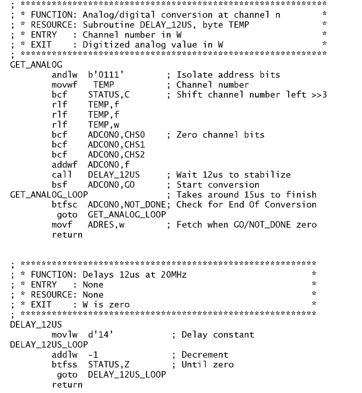
As an example, consider that we wish to read the channel n analog voltage (RAn) of a PIC16C74 and output the equivalent digital value at PortB. The main crystal is 20 MHz and VDD is to be used as Vref.
The listing of Program 14.1 assumes that the ADC module has been initialized at reset with startup code of the form:
which sets up the pin configuration according to the PCFGn settings of Table 14.3 to enable all eight ADC channels. The ADCON0 is initialized to ![]() to set the module clock source as the crystal frequency/32;
to set the module clock source as the crystal frequency/32; ![tmpA55_thumb[2][2] tmpA55_thumb[2][2]](http://what-when-how.com/wp-content/uploads/2011/06/tmpA55_thumb22_thumb.png) (giving a conversion time of
(giving a conversion time of![]() channel zero and the module is turned on. With an initial zero value of
channel zero and the module is turned on. With an initial zero value of![]() no conversion is actioned. The initial channel value is irrelevant.
no conversion is actioned. The initial channel value is irrelevant.
With the module initialized, the subroutine listed in Program 14.1 simply copies the contents of W, truncated to three bits for robustness, into a temporary location TEMP. There it is logic shifted left three places to align the channel number with the CHSn bits in the ADCON0 register.
Program 14.1 Taking a reading from channel n.
After clearing the CHS2:0 bits, the shifted channel number can then be added into ADC0N0 to set CHS2:0 to the appropriate channel.
Once the channel number has been set up, a 12 is delay subroutine is called and then the GO/DONE bit in ADC0N0 is set to initiate a conversion.7 The completion of the process can then be monitored by polling GO/DONE until this goes low. Notice that the p16c74.inc include file for clarity allows the programmer to use either bit name GO or NOT_DONE synonymously for bit 2. At this point the content of ADRES is the result of the conversion.
Rather than polling for completion, the end of conversion can be used to generate an interrupt. In particular if a conversion is to be done in the Sleep mode then this interrupt can be used to awaken the device.
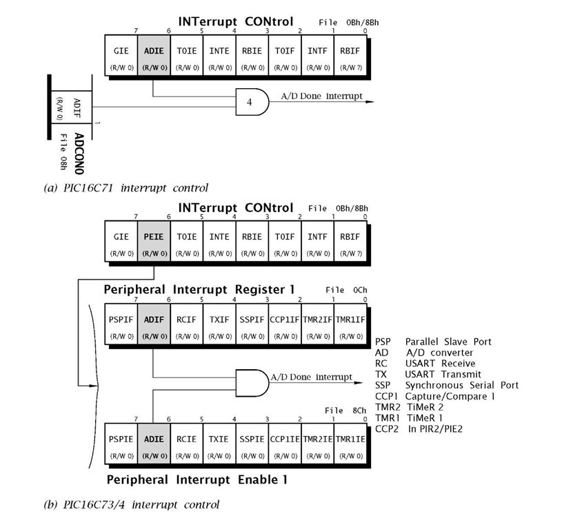
Fig. 14.10 Interrupt control for the ADC module.
The procedure in obtaining a digitized outcome using the ADC interrupt is similar to the polling technique.
1. Configure ADC module (see Table 14.3).
2. Configure ADC interrupt.
• Set the ADIE local mask bit to enable the ADC module interrupt.
• Clear the ADIF flag bit.
• Set the PEIE auxillary peripheral interrupt group mask bit (not the PIC16C71X line).
• Set the GIE bit to globally enable all interrupts.
3. Wait for the required acquisition time, typically 12 is.
4. Start conversion by setting the GO/DONE bit.
5. Continue……until interrupted.
6. Interrupt service routine (ISR) checks ADIF bit and if set reads the ADRES register and clears the ADIF bit.
7. For next conversion go to Step 2 or 3 as required.
To illustrate the process consider an interrupt-driven equivalent to the subroutine of Program 14.1, where we wish to action the digitization of the analog voltage at channel n. There are three considerations for this situation.
• Initialization code.
• The conversion subroutine.
• The interrupt service routine.
The initialization code depends a little on the target PIC device. The 18-pin footprint PIC16C71X line has a 4-channel ADC module as the counterpart to the PIC16F83/4′s Data EEPROM module. This can be seen by comparing the INTerrupt CONtrol register of the latter in Fig. 14.10(a) with the former shown in Fig. 7.4. Here the ADC module’s Interrupt Enable mask bit ADIE replaces the EEIE mask as INTCON[6] and the ADC module’s Interrupt Flag is located as ADCON0[1] (see Fig. 14.8).
The PIC16C73/4 28/40-pin line has a much larger line-up of peripheral devices and use two pairs of additional registers to service these auxil-lary4 interrupt mask and flag bits. These Interrupt registers are called the Peripheral Interrupt and Peripheral Interrupt Enable registers. PIR1 and PIE1 are shown in Fig. 14.10(b). The former at File0Ch holds eight interrupt flags, including ADIF at PIR1[6]. The latter at File 8Ch holds the corresponding mask bits. There is also a PIR2/PIE2 pair at File 0Dh:8Dh. Both these register pairs are enabled as a group by the PEIE (PEripheral Interrupt Enable) bit which takes the place of the single mask bit in INT-CON[6] in the 18-pin footprint devices. Thus in enabling the ADC module for interrupt handling, the programmer has to enable both the ADIE local and the PEIE group masks.
In our example, we assume a PIC16C74 target device. Then our initialization code might be:
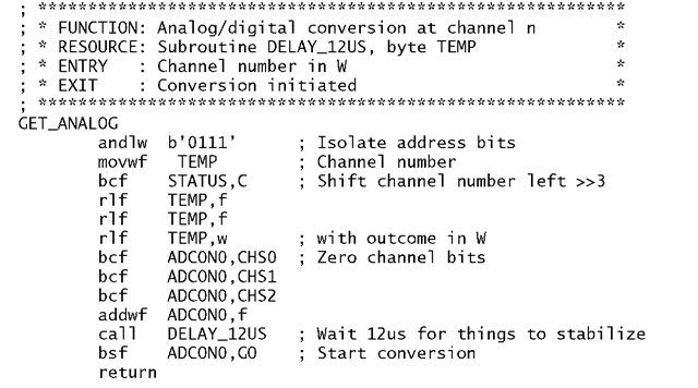
The interrupt-driven version of our subroutine shown in Program 14.2 is virtually identical to Program 14.1 except that the polling loop at the exit point is eliminated and, of course, no value is returned. However, the 12 is delay before commencing the process is still needed.
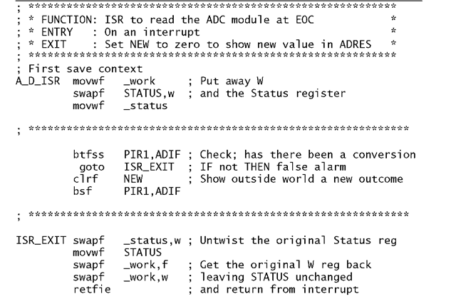
The ISR shown in Program 14.3 is entered when an interrupt (from any source) is generated. For simplicity we assume that there are no other sources of interrupt except from the ADC module. If this is the case, technically the check of the ADIF flag is redundant, although a spurious interrupt can never be ruled out. Where there are multiple sources of interrupt, then each flag can be tested in turn as shown.
In Program 14.3 a datum file register NEW is cleared to show the background program that the datum byte in ADRES has never been read. When the background routine fetches the digitized byte in ADRES it sets the flag byte NEW to a non-zero value. In a more sophisticated system a buffer of several digitized samples can he maintained by the ISR with NEW giving the number of samples in the buffer – see Example 14.1.
Program 14.2 Interrupt-driven subroutine to read channel n.
Program 14.3 The ISR for our interrupt-driven ADC software.
The core of the ISR is sandwiched by code to save and restore the Working and Status registers as described in Program 7.2. As the PIR1 register is available in both Banks 0 & 1, the more complex context saving code illustated in Program 7.4 is not required.
The ADC module can operate when the PIC is in its Sleep state. Indeed, a conversion during the (electrical) peace and quiet of sleep may well be preferrable than normal operation. When the ADC internal CR clock is used to sequence the analog module because the system clock is too low, then Sleep conversion is recommended as the CR and system clock are not synchronized and clock feed-through noise is a problem.
The following task list outlines the Sleep state conversion process.
• The ADC clock source must be set to CR, ADCS1:0 = 11.
• The ADIF flag must be cleared to prevent an immediate interrupt.
• The ADIE mask bit must be set to enable the ADC interrupt to awaken the processor.
• The GIE mask bit mask bit must be 0 unless the programmer wishes the processor to jump to an ISR when it awakens.
• The GO/DONE bit in the ADCON0 register must be cleared to initialize the conversion followed immediately by the sleep instruction.
• On awakening, the ADRES holds the digitized value.
Program 14.4 shows a Sleep state conversion, assuming that initialization code similar to the following has been executed.
This code shows the PIC16C71 as the target processor with its two PFCG1:0 bits set up to configure RA1:0 as analog inputs. The internal CR ADC module’s oscillator has been chosen as the clock source and ADC Interrupt flag ADIF (in the iNTCON register for the PIC16C71X line) cleared. Setting ADIE enables the ADC module’s interrupt system. Where applicable the PEIE mask bit at INTCON[6] must also be set. If these are not enabled, then entering the Sleep state will turn off the ADC module in the normal Sleep manner, although the ADON bit reamins 1, and the conversion is aborted. This will also occur if the CR clock option was not choosen.
Program 14.4 Digitizing Channel 1 of a PIC16C71 device.
Program 14.4 shows a conversion being implemented from Channel 1 (CHS1:0 = 01). After the channel has been set up and time allowed for settling5 the GO/DONE bit is cleared to start the conversion process. Where the CR oscillator option has been choosen, there is a 1-instruction cycle delay inserted to allow for the following sleep instruction to close down the processor.
After the PIC has awakened, the ADIF can be cleared and the digitized value read from the ADRES register.
As was the case for the other peripheral devices described in earlier topics, C code may be used to interact with the ADC module. The various configuration ports may be accessed in the same manner as at assembly level or, as in Program 14.5, the appropriate compiler built-in functions used to set up and manipulate the SPR control and status bits.
For our example we are going to code a 20 MHz PIC16C74 to act as a comparator in the manner of the Example 11.2. Here we want to compare the parallel-input 8-bit word N at Port B with the analog input at Channel 1. Outputs at RC2:0 are to represent Analog Lower Than N, Equivalent and Higher Than N respectively. The comparator is to have a hysteresis of ±1 bit. That is, if previous comparisons showed Analog < N then the trigger level is N + 1 for equality. Similarily, on a downward trajectory the trigger level is decreased to N — 1 for equality.
The function compare() of Program 14.5 assumes that initialization code of the form:
The key internal functions used here are:
Used to set up the channel number n in ADCON0, bits CHS2:0.
This function configures bits ADCS1:0 in the ADCON0 to select the module’s clock source; here the processor oscillator/32. The script ADC_CLOCK_INTERNAL may be used to select the internal CR oscillator.
This configures bits PCFG2:0 in ADCON1 to select which port pins are analog, which are digital and if an external Vref is to be used. The script RA0_RA1_RA3_ANAL0G indicates that port lines RA3 and RA1:0 are to be analog with an internal Vref with the rest being digital (PCFG2:0 = 100, see Table 14.3. The equivalent script using an external Vref at RA3 is RA0_RA1_ANAL0G_RA3_REF. Scripts appropriate to any aprticular device are stored in the corresponding header file, in this case 16c74.h. All devices with an analog module have scripts ALL_ANALOG and NO_ANALOGS.
Activates GO/DONE in ADCON0 and returns with the digitized value from ADRES when GO/DONE goes to 1.
Not explicitely an analog module function; this delays by n/s. The #use de1ay(c1ock=20000000) declaration is used by this function to give the delay appropriate for the processor clock frequency.
If the channel number remains constant and the compare() function is not called up at intervals less than the 12 is settling time (the normal situation) then de1ay_us(12); can be omitted.
Program 14.5 A digital/analog comparator with hysteresis.
The function compare() in Program 14.5 expects the value of the hysteresis, which here is either +1 or -1 (FFh). Internally this is called delta. After the ADC module is read, the digitized value analog is compared with the contents of PortB plus delta and the three PortC bits (RC2:0) set to their appropriate state.
![tmpA53_thumb[2]_thumb tmpA53_thumb[2]_thumb](http://what-when-how.com/wp-content/uploads/2011/06/tmpA53_thumb2_thumb_thumb.png)


![tmpA-60_thumb[2][2] tmpA-60_thumb[2][2]](http://what-when-how.com/wp-content/uploads/2011/06/tmpA60_thumb22_thumb.png)


![tmpA-63_thumb[2][2] tmpA-63_thumb[2][2]](http://what-when-how.com/wp-content/uploads/2011/06/tmpA63_thumb22_thumb.png)

![tmpA-65_thumb[2][2] tmpA-65_thumb[2][2]](http://what-when-how.com/wp-content/uploads/2011/06/tmpA65_thumb22_thumb.png)

