Given that digital microcontrollers are in the business of monitoring and controlling the real environment — which is commonly analog in nature — we need to consider the inter conversion between the analog and the digital world. Analog input signals need conversion to a digital equivalent, that is analog to digital conversion (ADC). Thereafter the digital patterns can be processed in the normal way. Conversely, if the outcome is to be in the form of an analog signal, then a digital to analog conversion (DAC) stage will be necessary.
Fig. 14.1 Analog world – digital processing.
Of these two processes, illustrated in Fig. 14.1, A/D conversion is by far the more complex. Some PIC devices, notably the PIC16C7XX and 12C67X lines, feature integral multi-channel A/D facilities. However, analog outputs require external circuitry to implement the D/A process.
In this topic we will look at the properties of analog and digital signals and the conversion between them as relevant to the PIC MCU. After completion you will:
• Understand the quantization relationship between analog and digital signals.
• Appreciate the need to sample an analog signal at least twice the highest frequency component.
• Appreciate how the successive approximation technique can convert an analog voltage to a binary equivalent.
• Be able to select the correct ADC clocking source and frequency.
• Be able to select the analog channel for conversion.
• Be able to configure I/O pins as either analog or digital.
• Be able to write assembly-level programs to acquire analog data using polling, interrupt-driven and Sleep techniques.
• Be able to code high-level C programs to interface to the analog module.
• Know how to interface in parallel to a proprietary DAC.
The information content of an analog signal lies in the continuously changeable worth of some constituent parameters, such as amplitude, frequency or phase. Although this definition implies that an analog variable is a continuum between in practice its range is restrained to an upper and lower limit. Thus a mercury thermometer may have a continuous range between, say, -10°C and +180°C. Below this the mercury disappears into the bulb. Above and the top of the tube is blown off!
Theoretically the quantum mature of matter sets a lower limit to the smooth continuous nature of things. However, in practice noise levels and the limited accuracy of the device generating the signal sets an upper limit to the resolution that processing needs to take account of.
Digital signals represent their information content in the form of arrangements of discrete characters. Depending on the number and type of symbols making up the patterns, only a finite totality of value portrayals are possible. Thus in a binary system, an n-digit pattern can at the most represent 2n levels. Although this grainy view of the world seems inferior to the infinity of levels that can be represented by an analog equivalent, the quantizing grid can be tailored to be fit for the accuracy of the task to be undertaken. For example, a telephone speech circuit will tolerate a resolution of around 1%. This can use an 8-bit depiction, which gives up to 256 discrete values — « 0.5%. A music compact-disk uses a 16-bit scheme, giving a one part in 65,636 grid — an « 0.0015% resolution.
From this discussion it can be seen that any process involving inter-conversion between the analog and digital domains will involve transition through the quantization state. Therefore we need to look at how this affects the information content of the associated signals.
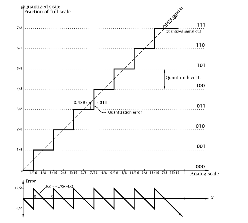
As an example, consider the situation shown in Fig. 14.2, where an input range is represented as a 3-bit code. In essence the process of quantizing a signal is the comparision of the analog value with a fixed number of levels – eight in this case. The nearest level is then taken as expressing the original in its digital equivalent. Thus in Fig. 14.2 an input voltage of 0.4285 of full scale is 0.0536 above quantum level 3. Its quantized value will then be taken as level 3 and coded as 011 b in our 3-bit system.
The residual error of -0.0536 will remain as quantizing noise, and can never be eradicated (see Fig. 14.3(d)). The distribution of quantization error is given at the bottom of Fig. 14.2, and is affected only by the number of levels. This can simply be calculated by evaluating the average of the error function squared. The square root of this is then the root mean square (rms) of the noise.
Fig. 14.2 The quantizing process.
The mean square is:
Thus the rms noise value of where L is the quantum level.
A fundamental measure of a system’s merit is the signal to noise ratio. Taking the signal to be a sinusoidal wave of peak to peak amplitude 2nL (see Fig. 14.3), we have an rms signal of that is
 Thus for a binary system with n binary bits, we have a signal to noise ratio of:
The dynamic range of a quantized system is given by the ratio of its full scale (2nL) to its resolution, L. This is just 2n, or in dB, 20 log 2n = 20n log 2 = 6.02n. The percentage resolution given in Table 14.1 is of course just another way of expressing the same thing.
Table 14.1: Quantization parameters.
| Binary bits
n |
Quantum levels (2W) | % resolution | Resolution Dynamic range | S/N ratio (dB) |
| 4 | 16 | 16.25 | 24.1 dB | 26.9 dB |
| 8 | 256 | 0.391 | 48.2 dB | 49.9 dB |
| 10 | 1024 | 0.097 | 60.2 dB | 61.9 dB |
| 12 | 4096 | 0.024 | 72.2 dB | 74.0 dB |
| 16 | 65,536 | 0.0015 | 96.3 dB | 98.1 dB |
| 20 | 1,048,576 | 0.00009 | 120.4 dB | 122.2 dB |
The exponential nature of these quality parameters with respect to the number of binary-word bits is clearly seen in Table 14.1. However, the implementation complexity and thus price also follows this relationship. For example, a 20-bit conversion of 1V full scale would have to deal with quantum levels less than 1 /V apart. Pulse-code modulated telephonic links use eight bits, but the quantum levels are unequally spaced, being closer at the lower amplitude levels. This reduces quantization hiss where conversations are held in hushed tones! Linear 8-bit conversions are suitable for most general purposes, having a resolution of better than ± 4%. Actually video looks quite acceptable at a 4-bit resolution, and music can just be heard using a single bit – i.e. positive or negative!!
S/N ratios presented in Table 14.1 are theoretical upper limits, as errors in the electronic circuitry converting between representations and aliasing (discussed below) will add distortion to the transformation.
The analog world treats time as a continuum, whereas digital systems sample signals at discrete intervals. Shannon’s sampling theorem1states that provided this interval does not exceed half that of the highest signal frequency, then no information is lost. The reason for this theoretical twice highest frequency sampling limit, called the Nyquist rate, can be seen by examining the spectrum of a train of amplitude modulated pulses. Ideal impulses (pulses with zero width and unit area) are characterized in the frequency domain as a series of equal-amplitude harmonics at the repetition rate, extending to infinity. Real pulses have a similar spectrum but the harmonic amplitudes fall with increasing frequency.
If we modulate this pulse train by a baseband signal A sin coft, then in the frequency domain this is equivalent to multiplying the harmonic spectrum (the pulse) by A sin Cft, giving sum and different components thus:
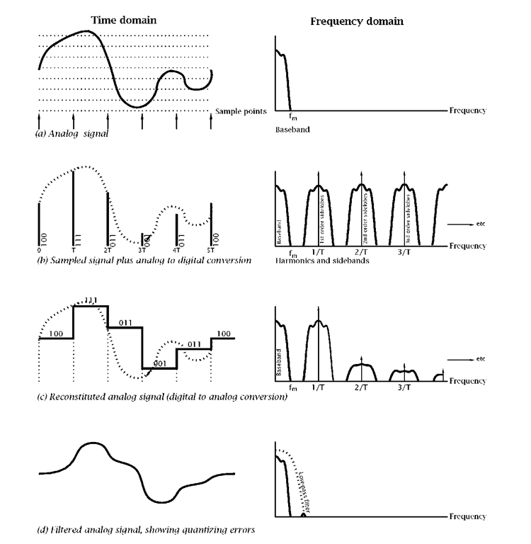
More complex baseband signals can be considered to be a band-limited (fm) collection of individual sinusoids, and on the basis of this analysis each pulse harmonic will sport an upper (sum) and lower (difference) sideband. We can see from the geometry of Fig. 14.3(b) that the harmonics (multiples of the sampling rate) must be spaced at least 2 x fm apart, if the sidebands are not to overlap.
A low-pass filter can be used, as shown in Fig. 14.3(d), to recover the baseband from the pulse train. Realizable filters will pass some of the harmonic bands, albeit in an attenuated form. A close examination of the frequency domain of Fig. 14.3(d) shows a vestige of the first lower sideband appearing in the pass band. However, most of the distortion in the reconstituted analog signal is due to the quantizing error resulting from the crude 3-bit digitization. Such a system will have a S/N ratio of around 20 dB.
In order to reduce the demands of the recovery filter, a sampling frequency somewhat above the Nyquist limit is normally used. This introduces a guard band between sidebands. For example the pulse code telephone network has an analog input bandlimited to 3.4 kHz, but is sampled at 8 kHz. Similarly the audio compact disk uses a sampling rate of 44.1 kHz, for an upper music frequency of 20 kHz.
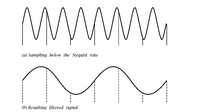
A more graphic illustration of the effects of sampling at below the Nyquist rate is shown in Fig. 14.4. Here the sampling rate is only 0.75 of the baseband frequency. When the samples are reconstituted by filtering,the resulting pulse train, the outcome – shown in Fig. 14.4(b) – bears no simple relationship to the original. This spurious signal is known as an alias. Where an input analog signal has frequency components above half the sampling rate, maybe due to noise, then this will appear as distortion in the reconstituted signal. For this reason analog signals are usually low-pass filtered at the input of an A/D converter. This process is known as anti-aliasing filtering.
Fig. 14.3 The analog-digital process.
The mapping function from an analog input quantity to its digital equivalent can be expressed as:
Fig. 14.4 Illustrating aliasing.
where ki is the ith binary coefficient having a Boolean value of 0 or 1 and Vin < Vref where Vref is a fixed analog reference voltage. Thus Vin is expressed as a binary fraction of Vref and the Boolean coefficients k-1 are the required binary digits.
To see how we might implement this in practice, consider the following successive approximation mechanical analogy. Suppose we have an unknown weight W (analogous to Vin), a balance scale (compare to an analog comparator) and a set of precision known weights 1, 2, 4 and 8gm (analogous to an Vref of 16 gm). A systemic technique based on the task list might be:
1. Place the 8g weight on the pan. IF too heavy THEN remove (k1 = 0) ELSE leave (k1 = 1).
2. Place the 4g weight on the pan. IF too heavy THEN remove (k2 = 0) ELSE leave (k2 = 1).
3. Place the 2g weight on the pan. IF too heavy THEN remove (k3 = 0) ELSE leave (k3 = 1).
4. Place the 1 g weight on the pan. IF too heavy THEN remove (k4 = 0) ELSE leave (k4 = 1).
will yield the nearest lower value as the sum of the weights left on the pan. For example if W were 6.2 g then we would have a weight assemblage of 4 + 2 g or 0110^ for a 4-bit system.
The electronic equivalent to this successive approximation technique uses a network of precision resistors or capacitors configured to allow consecutive halving of a fixed voltage Vref to be switched in to an analog comparator, which acts as the balance scale.
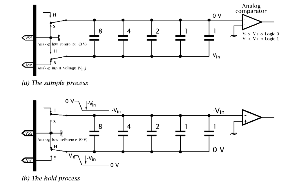
Fig. 14.5 Initializing the 8-4-2-1 capacitor network.
Most MCUs use a network of capacitors valued in powers of two to subdivide the analog reference voltage, such as shown in Fig. 14.5. Small capacitance values are easily fabricated on a silicon integrated circuit and although the exact value will vary somewhat between different batches of ICs, within the one device this value will closely match and track with changes in temperature and supply voltage. Multiples of the base value can be fabricated by paralleling unit devices – typically gate-source capacitance. The nominal value of a unit capacitor for a PIC16C7XX device is 0.2 pF giving a total capacitance of approximately 52 pF; that is 256 x 0.2.
Before the conversion process gets underway, the network has to be primed with the unknown analog input voltage Vin. This sampling acquisition process takes a finite time due to the charging time constant with the resistance of the external circuit together with internal pathways and switch plus a 5 is analog settling time. If the external resistance is 10 kQ, and internal resistance approximately 10kQ2, the time constant t is approximately 50 pF x 20 kQ = 1 /is.
2 It varies considerable with supply voltage and temperature.
To get to within 0.2% of the final voltage; that is 0.5 of an 8-bit quantum level error, takes approximately 7 x t. Taken with the 5 is settling time, the minimum sample time before starting a conversion is around 12 is. This can be lowered a little by reducing the source resistance. This resistance should not exceed 10 kQ as pin leakage IL =±1 / A will give a voltage offset approaching the quantum voltage step. Once charged, the sampling switches disconnect the input pin from the network to hold the voltage constant, so that voltage changes during the conversion period do not affect the outcome. Thus in a multi-channel ADC module, the channel selection can be changed at this time.
During the sample (S) period, the top capacitor electrodes are held to 0 V and bottom electrodes are charged to Vin. The change-over to the hold (H) position grounds the bottom electrodes and allows the top electrodes to float. The voltage across a capacitor can only change if charge is transferred across electrodes, AQ = CAV. Thus the change in voltage AV = —Vin at the bottom electrodes is matched at the top floating electrodes, which now become 0 — Vin, as charge cannot flow in or out of the floating top electrodes. Thus at the start of the conversion process the inverting input of the analog comparator is — Vin.


![tmpA-17_thumb[1] tmpA-17_thumb[1]](http://what-when-how.com/wp-content/uploads/2011/06/tmpA17_thumb1_thumb.png)

