However, at the same time the Change latch becomes transparent. When the reading action is over, the Change latch freezes and captures the pin state as it is at the time of reading. The outputs of both the Capture and Change latch are Exclusive-ORed together.An XOR gate detects differences between its two inputs. As the Capture latch is now transparent, any subsequent change at the pin input will cause the output of the associated XOR gate to go to logic 1. Each of the four PortB cells RB7:4 has a Change feature and the four XOR gates are ORed to give a composite signal which sets the RBIF (Register B Interrupt Flag) in the INTCON of Fig. 7.4.If the RBIE (Register B Interrupt Enable) bit is set then this is a convenient way of awaking a PIC slumbering in its Sleep state. If the GIE (General Interrupt Enable) bit is set as well, a change in the top nybble of Port B will cause an interrupt as well. Each XOR gate is ANDed with the TRIS line so that only bits that are programmed as an input can contribute to the Change signal.
Care must be taken in using this facility. For example, using the lower (non-change) part of PortB (e.g. bclr P0RTB,0) can affect the Change facility by forcing the latches to resample. Also a change may occur at the instant the port is being read and may be missed, although later A parts (e.g. PIC16C74A versus PIC16C74) altered the sampling logic to remove this latter problem. Neither of these foibles are factors if a keypad is used to awaken a sleeping PIC.
Once the PIC has responded to the Change interrupt the Change signal setting RBIF should be removed by reading Port B, which equates the state of the two D latches. Only then should RBIF be cleared. Failure to do this initial read will result in this interrupt flag being immediately set again.
As an example, using the keypad to awaken the PIC with the assumption that GIE is zero (no interrupt) should be implemented as:
Most PIC devices have relatively few I/O port lines - see Table 11.1. Even the larger footprint devices, such as the PIC16C74 with 33 peripheral pins, may not have enough parallel I/O resources for some projects, especially as several other peripheral devices may need to use the shared I/O pin budget.
As an example, consider a multi-purpose intruder alarm which can monitor up to eight zones- for example, floors in a multi-story building. Each zone can have up to eight movement sensors. A display of eight lamps back at base is to be used to indicate in which zone the intruder is located.
Based on this specification, a budget of 72 (64 input and 8 output) parallel I/O pins will be required. Rather than using one PIC device per zone reporting back to a main controller7 it has been decided to expand the I/O capabilities of a single PIC16F84 device.
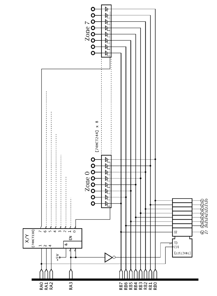
One expansion architecture is shown in Fig. 11.10. Here PortB is used to implement an external data bus which connects to the eight zone 3-state buffers and one indicator flip flop array. Each zone’s set of sensors are interfaced to this local bus via an octal 3-state buffer. One of eight buffers can be enabled using a 3 to 8-line decoder addressed from Port A. For example, if RA2:RA1:RA0 were 111 b and RA3 = 0 then Zone 7′s buffers are enabled and its eight sensors can be read in at Port B.
To activate the one output lamp array, RA3 should be logic 1 and Port B set to output. Data can then be clocked into the flip flop array by pulsing RA0 low then high to give a rising edge.
The number of output ports may be expanded in this architecture to eight by using a second 3 to 8-line decoder to select the port enabled 7An implementation that is perfectly feasible and cost effective; see SAQ 11.1.
Fig. 11.10 A multi-zone intruder alarm.
when RA3 = 1. However, up to two extra output ports could be added by simply substituting RA0 by RA1 and RA2 to enable these two additional flip flop arrays. For example, one port could show which sensor(s) within the zone was active and RA4 used to sound a buzzer if any zone was active.
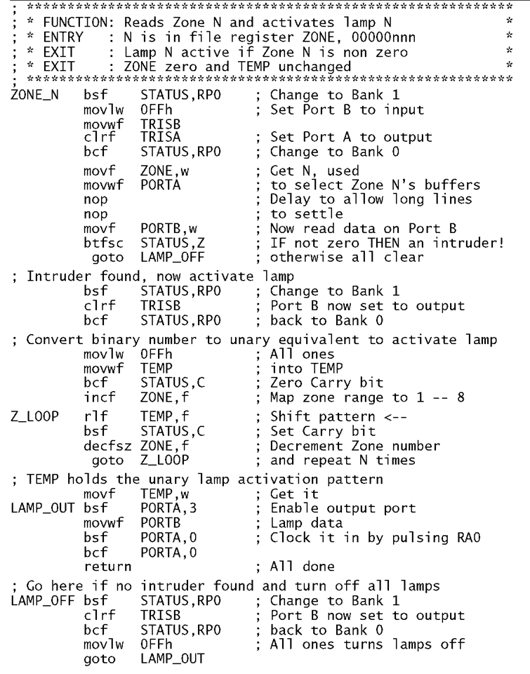
Program 11.3 Interacting with the intruder hardware.
To show how this hardware interacts with the software consider the subroutine in Program 11.3 below that reads Zone N and if non-zero then lights lampN; where N is an integer 0-7 in a file register called ZONE on entry. We assume that an active sensor gives logic 1 and a lamp illuminates on a logic 0.
Checking ZoneN is simply a matter of setting PortB up as an input port and sending the Zone N binary pattern to Port A. The 3 to 8-line decoder is enabled whenever RA3 is low, so no processing of the Zone binary code is needed. Due to the long connection lengths, a short delay is introduced to allow data to settle. For a real system, a delay of several hundreds of milliseconds and a digital smoothing routine, such as the debounce routine of Program 11.2, would be needed for reliable data acquisition, assuming that the zone buffers were geographically distant.
Activating the eight lamps is a little more tricky. In either case, PortB must be configured as an output. The lamps are then actuated by sending the appropriate pattern to PortB, bringing RA3 high and then pulse RA0. This is implemented in Program 11.3 in routine LAMP_OUT. The lamp datum is simply all logic 1 s where no intruder has been detected, that is where the sensor data has been read as all zeros.
When an intruder has been detected, then lamp N alone must be lit; for instance,![]() for Zone 6. To do this, the binary zone code in ZONE must be converted to the appropriate unary (one of n) code. For example, Zone 2 00000010b maps to
for Zone 6. To do this, the binary zone code in ZONE must be converted to the appropriate unary (one of n) code. For example, Zone 2 00000010b maps to![]() , Zone 3 00000011b maps to
, Zone 3 00000011b maps to![]() etc.
etc.
In the program the unary code is built up in file register TEMP, which is initially set to![]() . By clearing Carry before entering the loop at Z_LOOP but setting it to 1 within the loop, a single zero can be shifted left using the Rotate Left File instruction rlf TEMP,f. This gives the sequence
. By clearing Carry before entering the loop at Z_LOOP but setting it to 1 within the loop, a single zero can be shifted left using the Rotate Left File instruction rlf TEMP,f. This gives the sequence![]()
As this shift progresses, the ZONE datum (mapped to the range 1-8 so that at least one shift is implemented) is decremented and the loop exited when this reaches zero. Thus the position of the lone 0 (the initial C = 0) represents the original zone number. This unary code is then sent out to the lamp port at LAMP_OUT to activate the one-of-n indicator.
Examples
Example 11.1
A 2N3055 NPN bipolar transistor is to be used to activate the field coils of a small stepper motor. Taking into account the minimum gain of the transistor over the range +85 — -40°C, it has been calculated that the base current must be at least 10 mA. The transistor is to be controlled from a port pin and its base-emitter voltage can be assumed to be no more than 0.7 V and VDD is 5 V. What is the maximum value of the base resistor RB and given this value, what will be the worst-case maximum base current?
Solution
For currents of this magnitude we can assume that the pin voltage will be less than 5 V. The data sheet specifies a minimum voltage of 4.3 V (a drop of 0.7 V) for a Iqh of —3 mA but for currents greater than this we must resort to graphical techniques.
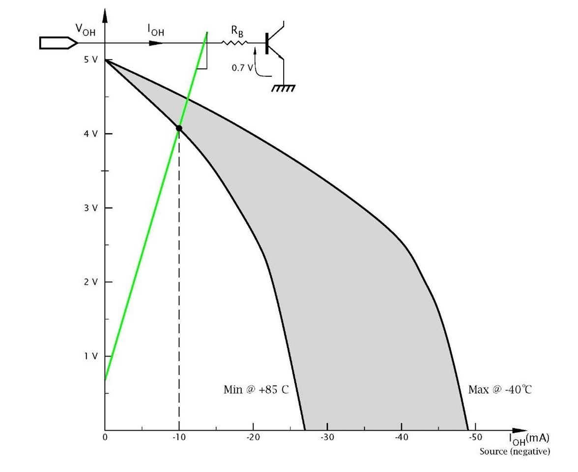
Figure 11.11 shows the graphical relationship of output source current IOH for a high output voltage state VOH. The grey area is bounded by the minimum situation, which is at +85°C and maximum condition at —40°C.
This voltage VOH is also a function of the transistor input base resistor circuit according to the equation VOH = 0.7 + IOH x RB. This straight line relationship (called a load line) is shown on the graph from (0,0.7) drawn to intersect the minimum locus at a current of —10 mA. This crossover is the only point that satisfies both current-voltage relationships. The slope of the load lineis the resistance in kQ (as current is in mA) and measures 280Q.![tmp9132_thumb[2]_thumb tmp9132_thumb[2]_thumb](http://what-when-how.com/wp-content/uploads/2011/06/tmp9132_thumb2_thumb_thumb.png)
Fig. 11.11 Source current against voltage.
Extending the load line onwards gives the maximum current as the X co-ordinate of the intersection with the Maximum locus, which is approximately 11.5 mA; not much different. If the current requirement had been larger, then the minimum/maximum currents diverge showing a significant temperature sensitivity. For example, a 20 mA minimum base current requires a base resistor of « 120Q (assuming a base voltage of 0.8 V) and the maximum base current would be 28 mA.
Example 11.2
An 18-pin mid-range PIC is to be used as a digital comparator where a parallel-input 8-bit word P is to be compared to a byte datum located in a file register named TRIP. Outputs are to indicate Lower-Than, Equivalent and Higher-Than. The comparator is to have an hysteresis of ±1 bit. That is, if previous comparisons showed N < TRIP then the trigger level is increased to TRIP + 1 for equality. Similarly, on a downward trajectory the equality level is to be decreased to TRIP – 1.
Datum P is to be input via Port B set up as input and the lower three Port A pins give the active-high comparator outputs <, ==, > at RA2, RA1, RA0 respectively.
Solution
The task list for such a specification is:
1. Subtract P from LEVEL.
2. IF Equal (EQwhen Z=1) THEN == output active.
3. ELSE IF P Higher than LEVEL (HI when C=0, Borrow) THEN > output active AND LEVEL = TRIP – 1.
4. ELSE IF P Lower than LEVEL (LO when C=1, No Borrow) THEN < output active AND LEVEL = TRIP + 1.
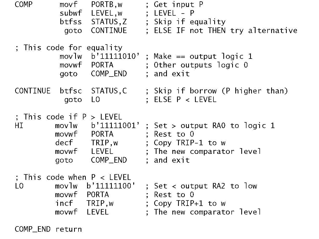
The subroutine given in Program 11.4 assumes that the main program has set up the port directions accordingly and the fixed value is in TRIP. Initially LEVEL would have been set to the same value as TRIP but would subsequently vary by ± 1 as per the specification – the hysteresis band.
Software solutions to traditional hardware functions, such as comparison, have the advantage of greater flexibility, albeit at the price of a lower data throughput. Using low-cost ‘computing engines’, such as the PIC, means that relatively simple functions traditionally implemented by dedicated hardware can be replaced by embedded processors.
In this instance, flexibility could be replacing the fixed trip level by a variable datum input via, say, Port C – requiring a larger footprint device; eg.PIC16C74 (see SAQ 11.7).Alternatively, an analog signal could represent one or both of the levels in devices with integral A/D converters – see Example 14.7. In all these situations the hysteresis may advantageously be made a fraction of the trip voltage, ![tmp9134_thumb[2][2] tmp9134_thumb[2][2]](http://what-when-how.com/wp-content/uploads/2011/06/tmp9134_thumb22_thumb.png) rather than a fixed ± 1 bit.
rather than a fixed ± 1 bit.
Program 11.4 A digital comparator with hysteresis.
Example 11.3
The principle of a stepper motor is shown in Fig. 11.12. In essence there are four coils, labelled A, B, C, D, which maybe selectively energized either singly or in pairs, to generate a magnetic field in one of eight directions in divisions of 45 °.4 Thus Coil A alone gives a northerly field, A & B together give a north-easterly direction, B alone is east, etc. The rotor follows the field as it changes direction provided that inertial considerations allow it to keep up during acceleration and de-acceleration.
Solution
Our first step is to devise a table showing energization patterns for the eight possible field directions, as shown in Table 11.2.
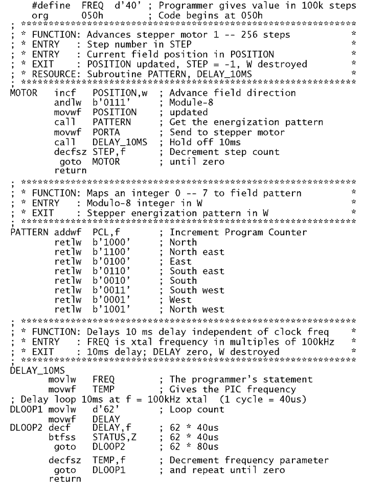
Program 11.5 Driving a stepper motor.
Table 11.2: Energization pattern for the eight field directions.
| Position | A | B | C | D | Bearing |
| 0 | 1 | 0 | 0 | 0 | |
| 1 | 1 | 1 | 0 | 0 | |
| 2 | 0 | 1 | 0 | 0 | |
| 3 | 0 | 1 | 1 | 0 | |
| 4 | 0 | 0 | 1 | 0 | |
| 5 | 0 | 0 | 1 | 1 | |
| 6 | 0 | 0 | 0 | 1 | |
| 7 | 1 | 0 | 0 | 1 |
The coding shown in Program 11.5 comprises three subroutines. MOTOR
The main subroutine simply modulo-8 increments the position vector by post-ANDing with 00000111b to give a wrap around from 7 to 0. This vector is then converted to the appropriate energizing pattern and sent out to the motor after a nominal 10 ms delay. The process is repeated until the decrementing STEP datum reaches zero – if initially zero then 256 steps will be actioned.

