The Parallel port is the most fundamental of the various input and output capabilities provided in a typical microprocessor- or microcontroller-based system. A parallel port enables up to n-bits of external data at a time to be directly read into the processor or sent out from the processor one byte at a time. The number of such parallel lines varies between members of the PIC family; those listed in Fig. 10.1 provide a minimum of five (8-pin devices) and a maximum of 33 (40-pin devices). Specifically in the PIC16F84 there are 13 input/output (I/O) lines, one of which is shared with the external interrupt and one with the Timer input. After reading this topic you will:
• Appreciate the function of a parallel input/output (I/O) port.
• Understand the structure of a parallel I/O port and differentiate between an active and passive pullup.
• Know how to configure an I/O port line.
• Comprehend how read-modify-write instructions interact with parallel I/O ports.
• Appreciate the electrical and power characteristics of an I/O port.
• Know how to enable weak pull-up resistors in PortB.
• Understand how the function of the interrupt on Port B Change operates.
• Be able to expand the number of I/O lines using external hardware.
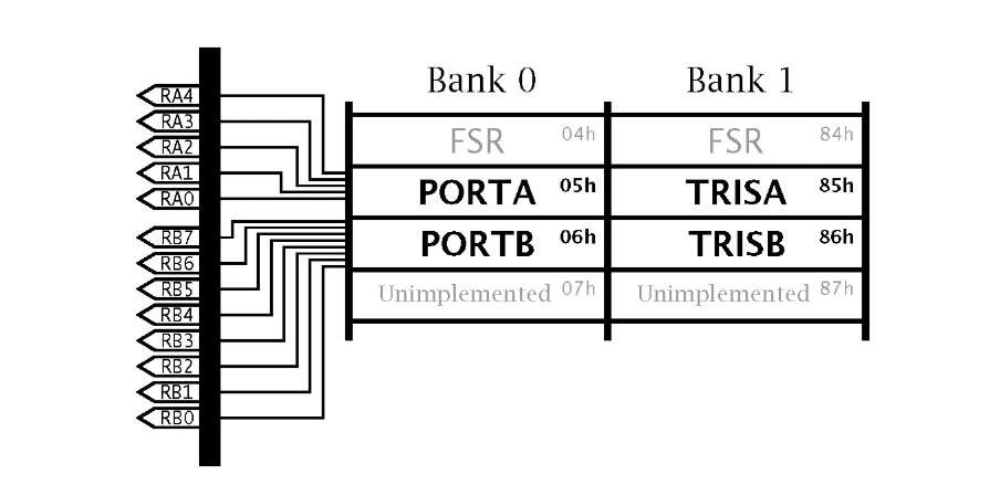
Conceptionally a parallel I/O port can be considered as a file register with its contents visible to the outside world. This somewhat simplified view is represented in Fig. 11.1, which is based on a magnified section of the PIC16F84 Data store shown in Fig. 4.6.All 18-pin footprint 14-bit core PICs have the 13 I/O lines depicted in Fig. 11.1.3 Mid-range 28-pin+ devices have an extra RA5 I/O line and additional ports as listed in Table 11.1. Such parts will have a larger repertoire of on-chip peripheral devices which share the parallel I/O lines, so the increased parallel I/O capacity may be largely illusionary. For example the PIC16C74 shares five of the Port A lines (RA5, RA3:0) and the 3-bit Port E as analog inputs to its 8-channel A/D converter.
Fig. 11.1 A boiled down view of the mid-range PIC 16CXX series Parallel Ports A and B.
Table 11.1: Summary of mid-range PIC parallel I/O provision.
Despite the depiction of Fig. 11.1, an I/O port does not behave quite like any other internal file register. For example, it has to be configured either to read the voltages on its associated pins (input) or to be able to write to these pins (output). Furthermore, we need to determine how this configuration interferes with the action of software that tries to alter or read the state of the port.
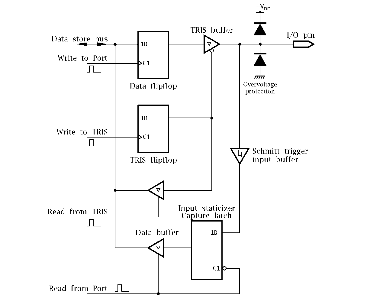
In order to understand the characteristics of parallel I/O ports we need to look at its hardware implementation. A somewhat simplified version of a single I/O port bit n together with its associated Data Direction bit is shown in Fig. 11.2. The two key elements in this circuit are the Data D flip flop and Data tri-state (3-state) buffer.
• Writing to this port will trigger the Data D flip flop and the data on the internal Data store line will be clocked in and held as long as the MCU is powered, see Fig. 2.15(c).For example:
Fig. 11.2 A simplified typical I/O port line.
will set all eight Data flip flops in Port B to logic 1. Setting the port bits will occur irrespective of whether such bits are configured as input or output. However, to pass the flip flop’s state through to the I/O pin, the TRIS (TRI-State) buffer must be enabled. In this situation, as shown in Fig. 11.3(b), the Data flip flop is directly connected to the outside world.
• Reading from this port enables the Data buffer and gates through the state of the staticizer latch2 to the internal Data store line. When the port is idling, i.e. not being read, the D latch is transparent and its output follows the state of the pin – see Fig. 2.15(a). When the port is being read, the D latch clock enable goes high and the data into the 3-state Data buffer is frozen, effectively holding its state constant while being read; that is staticizing it. The Data latch’s input is isolated from the I/O pin using a buffer with hysteresis (a Schmitt trigger) for noise immunity.3 For example, to read the state of PortB we have:
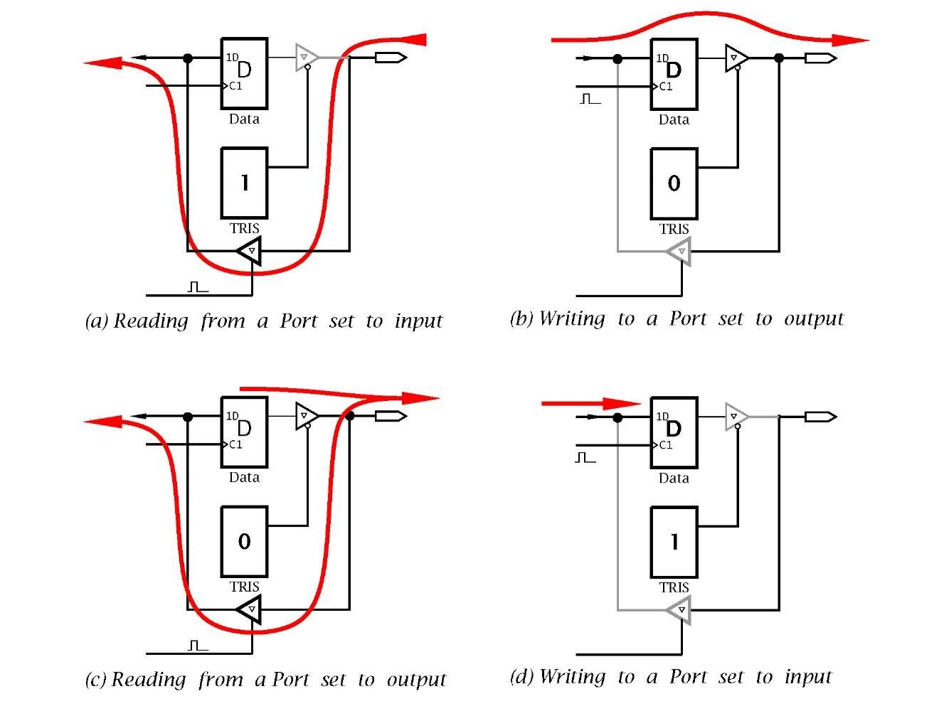
This reading action, shown in Fig. 11.3(a), will occur independently of whether the port line is configured as an input or output.
Each port I/O bit n has a shadow direction register bit n except Ports F & G which are always input. Thus Port A (File 05h) has TRISA at File 85h, PortB (File 06h) TRISB at File 86h, PortC (File 07h)/TRISC at File 87h etc. By setting TRISX[n] to 0, the corresponding PortX bit n’s TRIS buffer is enabled and the state of the Data flip flop gated to pin RXn; that is bit n is an output. Conversely if TRISX[n] is 1, then the TRIS buffer is disabled and pin RXn can be read without interference from the port’s Data flip flop; that is bit n is an input.
On resetting the PIC the TRIS registers are set to 1 to initialize all parallel I/O ports to inputs thus avoiding accidental damage which may occur if external devices are unintentionally switched on. However, resetting from a Sleep state leaves the port direction unchanged.
On the basis of our description, to set bits RB7:4 as outputs and RB3:0 as inputs we have in assembly language:
or in C assuming the definition: #define TRISB *(unsigned int *)0×86
The first generation PIC16C5XX series 12-bit core PIC devices have no explicit TRIS registers. Instead they use the tris instruction which copies the contents of the Working register to an internal control register that is not mapped into the Data store. Thus for our example:
When the 14-bit core devices were introduced with explicit TRIS registers, Microchip kept the tris instruction but did not guarantee that it would be implemented for future devices. However, many programmers still use tris and some C compilers, such as the CCS compiler, retain its use.
From Fig. 11.2 we see that a TRIS bit can be read from as well as written to. Although this may be rather useless, consider a programmer wishing to alter RB7 to an output (see Example 11.4).
bcf (Bit Clear File) is an example of a read-modify-write instruction whereby the state of TRISB is read into the processor, modified and then written out to TRISB. To do this the processor needs to both read and write to the file register.
Fig. 11.3 Reading and writing to a port bit set to input or output.
Because a parallel port may be configured as input, output or a mixture of both, it is important to know what restrictions are introduced when reading or altering the state of such special file registers. For example, what would happen if the software read from a port bit which has been configured as an output? The four possibilities enumerated in Fig. 11.3 are:
(a) Reading from a port set to input, TRIS = 1
Here the TRIS buffer is disabled and the state of the Data flip flop remains unchanged. For instance, movf 06h,w reads the state of Port B into the Working register.
(b) Writing to a port configured as an output, TRIS = 0.
Here the TRIS buffer is enabled and the Data flip flop altered by the processor writing to the port. The state of this flip flop appears on the I/O pin. For instance, movlw b’10101010′ movwf 06h sets the PortB I/O pins to 10101010b.
(c) Reading from a port configured as an output, TRIS = 0.
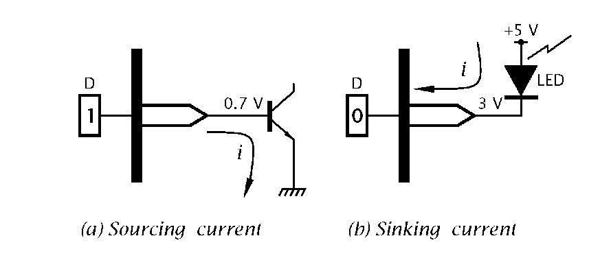
In this situation the TRIS buffer is enabled and so the I/O pin is connected to the Data flip flop. In most situations reading a port set to output will effectively copy the state of the flip flop into the CPU; however, this is not always the case. If the current taken by the device connected to the I/O pin is large the logic voltage at the pin may deviate significantly from the normal logic levels. For example, connecting a bipolar transistor directly to a port pin, as in Fig. 11.4(a), will take sufficient current from the TRIS buffer to drag the pin voltage to « 0.7 V, the forward conducting voltage of a typical transistor base-emitter.4
Fig. 11.4 Sinking and sourcing current.
The situation in Fig. 11.4(b) is similar with current flowing through the light-emitting diode (LED) into the port pin5 and the TRIS buffer will be pulled up to « 3 V assuming a conducting LED offset of 2 V. In these situations the outcome of reading a port pin set to output is often not the state of the port bits’ Data flip flop. Thus for example, btfsc PORTB,7 in purporting to skip if bit7 of PortB is zero may fail to function as expected if that bit is set to output and pin RB7 is sinking or sourcing too much current. (d) Writing to a port configured as an input, TRIS = 1.
In this situation the state of the Data flip flop will be altered in the proper manner. However, as the TRIS buffer is disabled, any change will not be reflected at the I/O pin until the direction of the port pin is subsequently changed to output.
This ability to set up the state of a port in a manner invisible to the outside world is important when the PIC is reset. On reset, all ports are set to input, in other words all TRIS ports are set to FFh. Any ports that are to control devices in the outside world should first be written to with the initial state of these devices and only then changed to output. For example, if four electromagnetic relays are connected to port bits RB7:4 and are to be energized after reset by logic 1 states on their input we have:
where we are assuming that the lower four Port B bits are to remain in their input state.
In item (c) we referred to current into (known as sink current) or out of (known as source current) the port pin. In most situation a port pin configured as an output will only be required to source or sink a few milliamps of drive current. Nevertheless, it is important to be aware of the drive capabilities of port output pins.
Generally two situations are tabulated in a device’s data sheet.
1. Sink current IOL when an output is logic 0 should not exceed +8.5 mA if the low voltage VOL is not to rise above 0.6 V.
2. Source current from a logic 1 output IOH should not exceed -3 mA if the high voltage is not to drop more than 0.7 V below VDD. The negative current denotes source; i.e. out of the device.
Larger currents may be sourced or sunk, as in Fig. 11.4, if degradation of logic levels are acceptable, subject to an absolute limitation that it must be within the range -20 —► +25 mA for any single I/O pin to avoid damage. Where more than one I/O pin is involved in driving current, an overall global limit must be observed. For example, the 18-pin PIC16F83/4 limits Port A to -50 — + 80 mA and PortB to -100 — + 150 mA in total. 100 mA is the global maximum current IDD into the VDD pin and 150 mA the global maximum out of the VSS pin. Bigger packages, such as the 40-pin PIC16C74, support larger global currents with a corresponding maximum IDD of 250 mA and ISS of -300 mA.


