Bits SSPCON[3:0] are the Mode control bits which set the communication protocol and various Master/Slave options as listed in Table 12.1. Of interest to us is the internal clock source in the SPI Master mode and the use of the SS pin when in the SPI Slave mode.
Finally, SSPCON[7] is the Write Collision (WCOL) status bit – not in SSPSTAT due to lack of space. This is set to 1 if the software writes to SSPBUF before the transmission of the previous byte has been completed. If set, it should be cleared by software to reset this warning mechanism.
Using Figs. 12.9 and 12.10 as a programmer’s model we can now deduce the hardware-software interaction in order to action a transmission of a byte and/or receive a new byte:
1. Configure SSP module.
• Set up SCK/RC3, SDO/RC5 as outputs and SDI/RC4 as an input (TRISC[5:3])
• Set up Master/Slave mode with appropriate clock source (SSPCON[3:0])
• Choose active TX clock edge with CKP (SSPCON[4])
• Enable the SSP by setting SSPEN (SSPCON[5])
2. Move datum to SSPBUF to initiate transmission.
3. IF WCOL = 1 THEN reset WCOL and go to item 2
4. Poll BF for 1 (SSPSTAT[0])
5. Move RX data from SSPBUF, which also resets BF
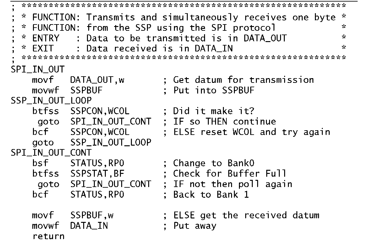
To illustrate this process, consider a subroutine SPI_IN_OUT which combines the function of SPI_READ and SPI_WRITE; that is it transmits the datum in file register DATA_OUT whilst at the same time returning the consequential received byte to DATA_IN.
Table 12.1: The SSP Mode bits.
SSPM[3:0]: Synchronous Port Mode select bits
The implementation of this subroutine depends on setting up the SSP during the initialization phase of the main software after Reset. In the following code fragment we are using the Fosc/4 clock rate Master mode:
The coding shown in Program 12.4 follows the task list exactly. Data to be transmitted is moved from the designated file register to SSPBUF and status bit WCOL checked to see that it got there. If there was a transmission in progress then the datum is not stored in SSPBUF and WCOL is set. If this subroutine is the only code to access the SSP then this should rarely be the case and in most instances this check is omitted, but its inclusion makes the system more robust.
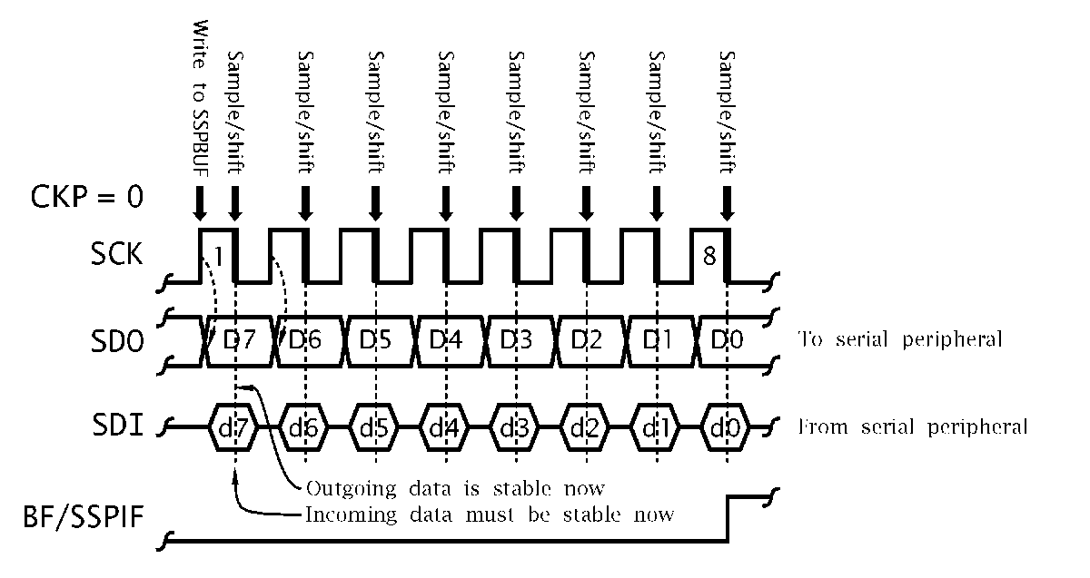
Once the transmit datum is in situ, the transmit sequence is immediately initiated, as shown in Fig. 12.11 and progresses to its conclusion. Once the Buffer Full status flag BF is set, the received datum can be moved out of SSPBUF to its ordained location. This automatically resets BF.
Program 12.4 Using the SSP for SPI data input and output.
Apart from a slight reduction in the code length, the advantage of using this hardware is the increase in speed. The actual transmit/receive takes eight SCK cycles, which in our case is eight instruction cycles. With an Fosc of 20 MHz the clocking rate is 5 MHz (that is a bit rate of 5 million bits per second, commonly written as 5 Mbit/s or 5 Mbps), giving a total time of 1.6 us per byte.
If speed is of the essence then the SSP can be interrupt driven, as the SSPIF in the PIR1 register is set at the same time as BF. If the SSPIE mask bit in the PIE1 register is set, together with the overall mask bits GIE and PEIE in INTCON, then an interrupt will be generated when the outgoing byte has been transmitted and the new incoming byte is ready and waiting in SSPBUF. The function of these bits are shown in Fig. 14.10. This interrupt can be used to awaken the PIC when in its Sleep mode.
Figure 12.11 shows the SPI mode timing for our subroutine. As we have cleared CKP then SCK is idling low. As soon as SSPBUF is written to, SCK goes high and the MSB of the TX datum appears at SDO. On the following edge, the MSB of the received datum is read in at SDI.
With this chosen polarity there is plenty of time for data from the external serial input port to present data to the PIC assuming that (as is usual) the its shift register is _/ triggered. This data is then sampled by the PIC on the following ^ of SCK, as indicated the the I sample/shift points in Fig. 12.11. However, as we see, data that the PIC places on its SDO pin is placed on the _/ of SCK ready and stable for the following active . This means that the serial output port must be negative-edge triggered to ensure that it shifts in stable data. To get around this problem an inverter should be inserted at the peripheral’s input shift register clock, effectively converting it to a negative-edge triggered shift register. Some more advanced SSP modules, such as included in the PIC16F87X line, allow the input sample time to be shifted to remove the need for this additional hardware.
Fig. 12.11 SSP SPI-mode master waveforms.
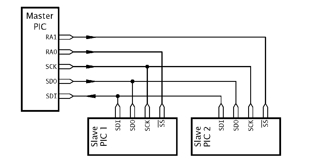
One use of serial transmission is to connect a number of PICs (or indeed other MCUs) together in one multiprocessor network. For example, a robot arm may have a MCU controlling each joint, communicating with a master processor. A simple multidrop circuit of one Master and two slave processors is shown in Fig. 12.12.
Fig. 12.12 A multidrop SPI communications network.
In this configuration the Master PIC externally drives the SCK of both Slaves, thus controlling when and how fast transmission occurs across the network. Both Slaves are configured in Mode6 (SSPM[3 : 0] = 0110) so that the Slave Select inputs are enabled. Thus, if the Master wishes to read a datum from Slave 2 the the latter’s SS is brought low and the Master clocks the eight bits from Slave 2′s SSPBUF/SSPSR, into its own SSP-BUF/SSPSR. At the same time any data transmitted by the Master will be received by the Slave. Slaves can rest in Sleep mode while all this is going on and the resulting interrupt used to awaken it after the transaction has completed provided that the PEIE and SSPIE mask bits are set.
SPI transactions may be coded in C either by mimicking the assemble-level code and setting/reading the appropriate registers, or by using built-in functions specific to the task. For example, for the CCS compiler constructions like:
effectively mimic our SPI_IN_OUT subroutine.
To illustrate this technique, consider our interface to the MAX549A coded in Program 12.3. In order to do this the SSP needs to be configured using code of the form:
has already been executed.
The MAX549A’s![]() is connected to Port A’s RA2 pin, and is identified in the setup code using the #bit directive, as described. With this definition in mind, the code in Program 12.5 simply comprises four
is connected to Port A’s RA2 pin, and is identified in the setup code using the #bit directive, as described. With this definition in mind, the code in Program 12.5 simply comprises four![]() calls with CE being pulsed between
calls with CE being pulsed between![]()
pairs. The function may be called with an evocation something like ![]()
Program 12.5 Interfacing to the MAX549A in C.
The key CCS compiler internal functions used for the SSPort in its SPI mode are:
This function configures the SSP as an SPI Master, with clock polarity rising edge and a +4 clock frequency. These scripts, and others such as spi_s1ave are part of the included header file 16c74.h. This function also sets the direction of the appropriate Port A and PortC pins.
Used to write out the value from the SSP. Checks that the BF flag is set before returning.
Virtually identical to spi_write() except that it returns the value read by the SSP. If a value is passed to this function then it will be clocked out of SDO.
Returns non zero if a datum has been received over the SPI connection, that is if BF is set.
Although the SPI protocol is relatively fast, it requires a minimum of three data lines plus one select line for each Slave device. Apart from the cost, adding a device to an original design will require some hardware modification. By increasing the intelligence of the Slave device, it is possible to send both control, address and data in the one serial stream. The Inter-Integrated Circuit (I2C)5 protocol developed by the Philips/Signetics Corporation in the early 1980s embodies this concept and also reduces the interface to only two lines by permitting bidirectional transmission.
SCL
The clock line sychronizing data transfer, serving the same function as SCK in the SPI protocol. However, SCL is bi-directional to allow more than one Master to take control of the bus at different times.
The original I2C specification set an upper limit on shift frequency of 100 kHz, that is 100kbit/s, but the specification was augmented in 1993 with a Fast mode with an upper data rate of 400 kbit/s, which is the current de facto standard. In 1998 a compatible High-Speed mode was added with an upper bit rate of 3.4 Mbit/s.
SDA
The I2C data line allows data flow in either direction. This bi-directionality allows communication from Master to Slave (Master-Write) or from Slave to Master (Master-Read). Furthermore it allows the receiver to signal its status back to the transmitter at the end of each byte.
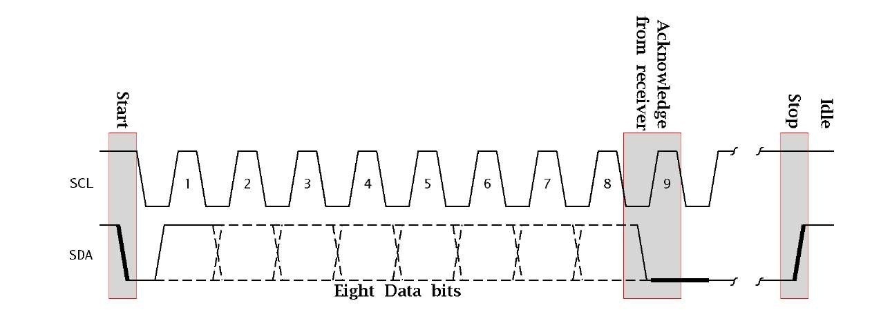
The I2C protocol is relatively complex and its full specification can be viewed at the Philips/Signetics Corporation web site6. Before looking at the basic protocol, we need to examine the SCL and SDA lines in more detail. When no data is being transmitted, both lines should be high; the Idle condition. A device wishing to seize control of an idling bus must bring its SDA output low. This is known as the Start condition. In order for the would-be Master to be able to pull this line low all other devices hung on the line must have their SDA pins open circuit and the line as a whole pulled up high through a single external resistor – see Fig. 12.14(a). To implement this SDA (and also SCL) outputs must be open-collector or open-drain – see Fig. 2.2. This means that any device hung on the bus is able to pull its line low by outputting a logic 0.
After the Start condition the Master then sends eight bits of information synchronized with eight clock pulses. During this period any changes in data on SDA must occur when the clock is low. Data can then be clocked into the slave on the following SCL rising edge. This data may represent address, control or information bits.
![tmp9209_thumb[2]_thumb tmp9209_thumb[2]_thumb](http://what-when-how.com/wp-content/uploads/2011/06/tmp9209_thumb2_thumb_thumb.png)


![tmp9213_thumb[2]_thumb tmp9213_thumb[2]_thumb](http://what-when-how.com/wp-content/uploads/2011/06/tmp9213_thumb2_thumb_thumb.png)
![tmp9214_thumb[2]_thumb tmp9214_thumb[2]_thumb](http://what-when-how.com/wp-content/uploads/2011/06/tmp9214_thumb2_thumb_thumb.png)


