Up to this point our microcontroller material has been presented piecemeal. To complete our study we are going to put much of what we have learnt to good use and design both the hardware and software of an actual widget (gadget). This is not an easy task to do in a single short topic. However, very little new material needs to be presented at this point, rather a process of coalescence.
We begin with our specification. Students invariably talk too long during their oral presentations. It is proposed that a dedicated embedded microcontroller-based system be designed to act as a time monitor. This monitor should default to a time-out of 10 minutes, but will have the provision to vary the allotted time from 1 to 99 minutes.
Once triggered, the monitor should perform the following sequence of operations:
1. When the GO switch is closed, a green lamp will illuminate and a dual seven-segment display will show a count-down from the timeout value to![]() at one-minute intervals.
at one-minute intervals.
2. After a further minute, an amber lamp only will illuminate, the count of![]() will be displayed and a buzzer will sound for nominally one second.
will be displayed and a buzzer will sound for nominally one second.
3. After a further minute, a red lamp only will illuminate together with a display of![]() The buzzer will sound for two seconds.
The buzzer will sound for two seconds.
4. Finally, after another minute the display will show![]() the red lamp will continue to be illuminated and the buzzer will sound continuously until the STOP switch is pressed. This will halt the timer and turn off all displays, lamps and buzzer. Indeed, closing the STOP switch at any time during the sequence above will cause the system to permanently halt. The system may be restarted from the time-out value by resetting the processor.
the red lamp will continue to be illuminated and the buzzer will sound continuously until the STOP switch is pressed. This will halt the timer and turn off all displays, lamps and buzzer. Indeed, closing the STOP switch at any time during the sequence above will cause the system to permanently halt. The system may be restarted from the time-out value by resetting the processor.
5. At any time the sequence can be frozen by toggling the PAUSE switch. When toggled again, the sequence will continue on from where it left off.
6. In order to alter the time-out from the default value of![]() , the SET switch must be closed when the system is reset. The display will then show
, the SET switch must be closed when the system is reset. The display will then show![]() and will count down slowly. The value showing when the SET switch is released will be the new time-out and will be retained indefinitely until another set process.
and will count down slowly. The value showing when the SET switch is released will be the new time-out and will be retained indefinitely until another set process.
The first decision to be made is the choice of microcontroller (MCU). In this case we are constrained by the need to use our topic’s model device, i.e. one of the mid-range PIC family. As we require non-volatile storage to store the time-out value we are limited at the time of writing to the PIC16F8X and 16F87X lines of devices to avoid the necessity to use an external serial EEPROM. As the display will physically be large for long-distant viewing the bulk of the circuit is not critical so the cheaper PIC16F84 device is our choice. The 18-pin count of this device compared to the alternative 40-pin PIC16F874 will require additional support functions to expand the port pin budget, but should better illustrate the tradeoffs of more complex systems.
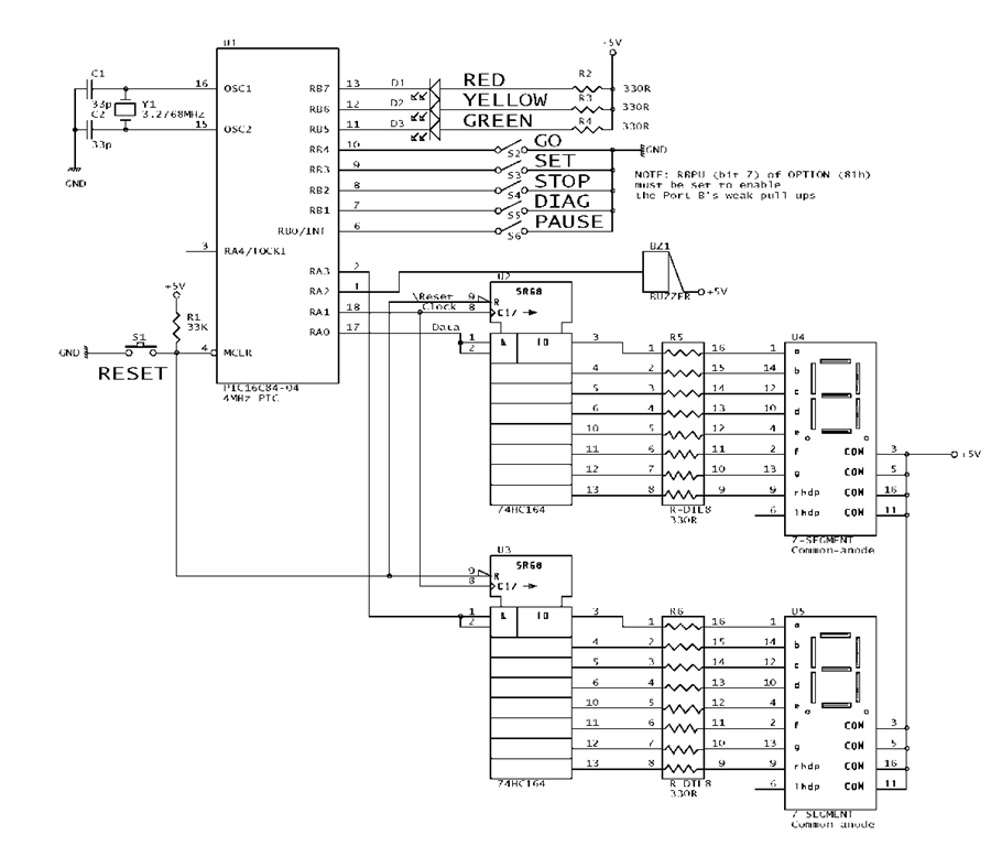
Based on this decision the final target hardware is shown in Fig. 16.1. The port pin budget is allocated as follows:
Fig. 16.1 The annunciator hardware.
Switches
The five switches S2…S6 implementing the functions GO, SET, STOP, DIAG, PAUSE are read from PortB at RB[4:0]. By using this port’s internal pull-up resistors (see Fig 11.7) no external resistors are required.
S1 with R1 provides a Manual reset in order to restart the count. This MCLR signal also provides a Reset signal feed for external circuitry.
All six switches can be conveniently implemented as momentary contact keyboard switches.
Lamps
Three suitably colored 10 mm (0.4″) high-brightness LEDs D3…D1 driven from RB[7:5] provide the light signals. 330Q series resistors limit the current to nominally 10 mA.
Buzzer
The buzzer should be a miniature solid-state device. A typical piezoelectric implementation will operate over a wide d.c. voltage range of typically 3-16 V and require little more than 1 mA at 5 V.8The buzzer is driven via RA2.
Numerical display
Two 7-segment displays give the required 2-digit read-out, facilitating the maximum specified period of 99 minutes. As only four port pins remain, a serial interface is implemented. This is similar to that shown in Fig. 12.2 but each SIPO shift register has a separate data feed, with RA0 being used for the ten’s digit and RA3 for the units digit. Both digits can therefore be simultaneously updated with eight shifts.
The common-anode seven-segment display pinning shown in the diagram is that of the 16-pin Dual In Line (DIL) footprint with both left and right decimal points – Ihdp and rhdp. Only the latter is used here (to indicate that the system has paused) in conjunction with the 8-bit 74HC164 shift register. Alternative 16- and 14-pinouts are commonly available and even dual-digit packages. However, even the 16-pin footprint pinout is not standardized.
Smaller-sized displays, typically below 0.8″/20 mm, use a single LED for each bar, with a conducting voltage drop of around 2 V.9 The DIL 330 Q series resistors R5 and R6 limit the current to around 10 mA. The common anodes are connected directly back to the normal +5 V power supply to avoid current surges affecting the logic circuits, and should be decoupled by small tantalum capacitors. Although the displays are normally rated for 20 mA, restricting the current to this value gives sufficient illumination and means that the 74HC164 shift registers do not need current buffering.10
Crystal
A 3.2768MHz crystal provides the timing for the MCU’s clock oscillator, giving an instruction rate of 819.21 kHz. A typical crystal of this value has a tolerance of ±30ppm and temperature coefficient of ±50ppm.
This unusual choice is 216 x 50 so if we use the 8-bit Timer 0 with a prescale value of 1:64 then we can create an interrupt 50 times per second. An alternative low-power configuration would be to use a 32.768 kHz crystal and generate an interrupt every two seconds. However, compared to the current consumption of the optical components, the MCU’s power dissipation is minor.
With the hardware environment designed, we can now concentrate on the software.
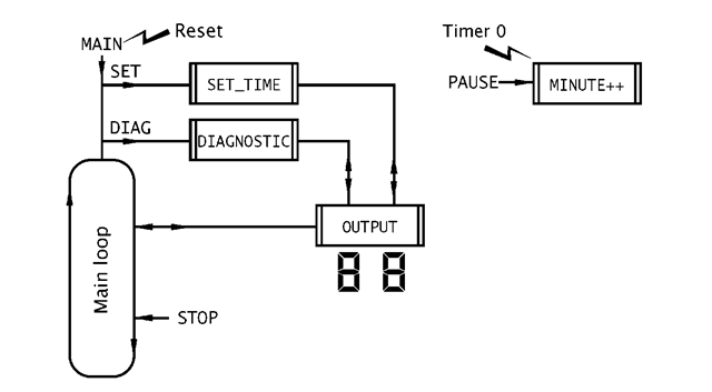
Fig. 16.2 The modular software structure.
Figure 16.2 shows the basic modular structure for our system. Here the distinctive double right/left edged box denotes a subroutine or Interrupt Service Routine (ISR). Three distinct processes can be identified together with two major supporting tasks.
Time base task
All processes are time related. Timekeeping is implemented in hardware by generating an interrupt 50 times each second. By keeping a Jiffy count, seconds and minute tasks are updated and are used to sequence the appropriate process.
By monitoring the PAUSE switch this decrementing time chain can be by-passed, hence freezing the countdown for as long as necessary.
Display task
All processes need to output the state of the count or status information to the two 7-segment displays. As this involves parallel to serial conversion and shifting, the task is better gathered into one module.
Main process
The Main process is a loop displaying the Minute count until it reaches zero, with a premature break if the STOP switch is closed.
Set-time process
If the SET switch is closed when the PIC is reset then the SET_TIME subroutine quickly decrements the display count until the switch is released. This displayed value is then written into Data EEPROM and is used by all subsequent Main processes as the starting value for the Minute count.
Diagnostic process
If the DIAG switch is closed on reset, the system enters a diagnostic subroutine. The essentially exercises each peripheral device in a manner calculated to ease hardware fault finding.
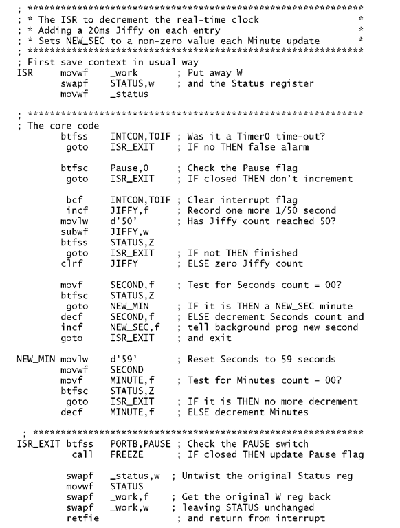
All processes are dependent on the Timebase task to pass basic realtime clock information back. As shown in Program 16.1 this is interrupt driven and is based on the Timer 0:Prescaler dividing down the 3.2763 MHz crystal-driven oscillator to give overflow every 50 s. As can be seen in Program 16.3, the Timer 0 interrupt is enabled and thus the PIC will enter ISR whenever the timer overflows – every 256 outputs from the Prescaler. Remembering that the crystal oscillator runs at 4 of the crystal frequency, a prescale ratio of 1:64 will give a timebase rate of 50 per second
The task list for this function is:
1. IF PAUSE switch open THEN
(a) Decrement the time chain by one Jiffy.
(b) IF new second THEN flag it.
2. ELSE
(a) Toggle the Pause flag.
(b) IF set THEN tell the world that the system is paused.
(c) ELSE display time to indicate normal running.
(d) Wait until PAUSE switch is released.
3. Return from interrupt.
Program 16.1 The timebase software.
Program 16.1 The timebase software.
From Program 16.1 we see that time is kept as a 3-byte count chain using file registers MINUTE, SECOND and JIFFY to hold the total. Assuming that the state of bit0 of file register Pause is 0, then one is added to the Jiffy count. Normally the ISR then exits but when Jiffy reaches 50 it is reset to zero and the Seconds count decremented. The file register NEW_SEC is also made non zero to indicate to background software that a second has elapsed. In the situation where the Second count reaches zero then it is reset to 59 and the Minute count decremented. The procedure is similar to the incrementing count of Example 7.4.
The Timebase task also handles the Pause function. The simplest approach would be to skip over the time decrement code if the PAUSE switch is closed. However, the necessity to keep the switch closed could be irksome if the period was more than a few minutes.
Implementing a push-on push-off scenario is ergonomically superior and can be more economically implemented in software rather than using a different type of switch compared to the others. In Program 16.1 the Pause handling code is located in the separate subroutine FREEZE. It is permissible to call a subroutine from an ISR in the same manner as calling one subroutine from another; that is nesting. The 8-deep hardware stack allows nesting up to eight deep. In our situation only two of the stack locations are used, allowing up to six calls deeper into the stack.
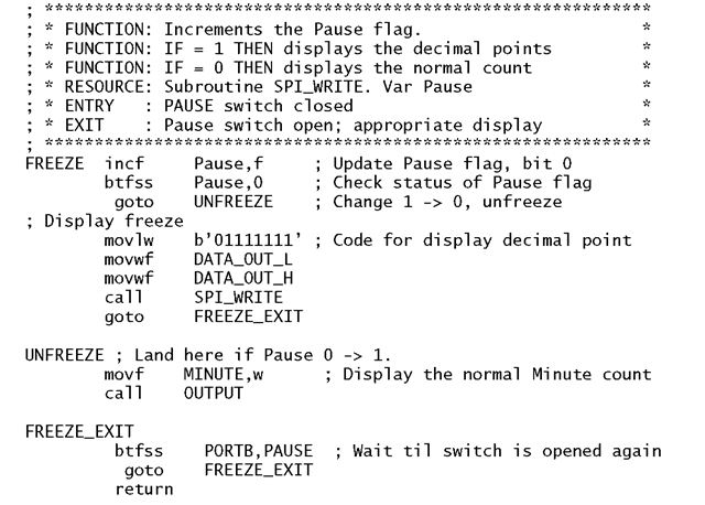
Subroutine FREEZE is only entered if the PAUSE switch is closed. On each entry the value of bit0 of the file register Pause is toggled. This is implemented by simply incrementing file register Pause.
Once Pause[0] is toggled, its state is tested and if 1 the pattern to only illuminate the two decimal points is sent to the SPI_WRITE subroutine. This is an arbitrary indicator display, another possibility would be![]() If Pause[0] is 0 then the state of the Minute count is sent to the OUTPUT subroutine and indicates to the user that the Pause function has ended.
If Pause[0] is 0 then the state of the Minute count is sent to the OUTPUT subroutine and indicates to the user that the Pause function has ended.
Finally, the subroutine does not exit until the user releases the PAUSE switch. This is important, as on exit the ISR will be re-entered again at the next Timer 0 overflow, and this would cause Pause to be repeatedly retog-gled. Some measure of switch debounce is obtained by zeroing Timer 0 and the Prescaler when the switch is released. This means that the switch will not be retested for a whole 50 second. It is for this reason that T0IF is cleared on exit from the ISR rather than at the more conventional entry point.
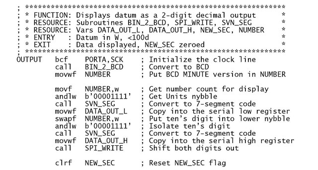
The task displaying the contents of the Working register in decimal is handled by the subroutine OUTPUT in Program 16.2. The task list for this function is:
1. Convert the binary datum to 2-digit BCD.
2. Convert both digits to 7-segment.
3. Serially shift out both bytes to the appropriate display.
Program 16.2 The data display function.
Program 16.2 The data display function.
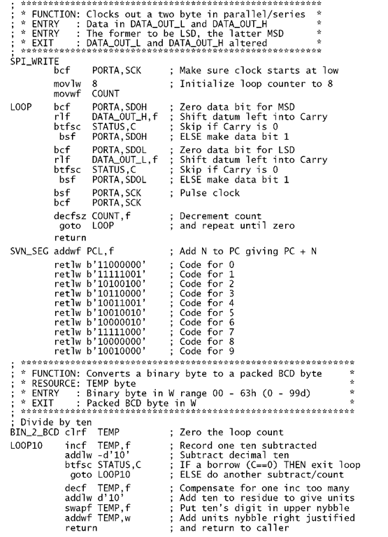
Subroutine OUTPUT listed in Program 16.2 follows the task list calling up the following utility subroutines. Binary to BCD conversion Subroutine BIN_2_BCD repetitively subtracts ten from the binary datum in the manner described in Program 5.9.Assuming that this datum is never greater than decimal 99 (63 b) then this count gives the ten’s digit. The residue is the unit’s digit. The two nybbles are packed together and returned in W. Binary to 7-segment decoder
Subroutine SVN_SEG converts a single datum nybble in W to its 7-segment coded equivalent as described in Program 6.4.
