NANODIAMOND STRUCTURES
Nanodiamonds that are produced under those very different conditions of atmosphere, temperature, and pressure have similar size distributions. In particular, extraterrestrial nanodiamonds, detonation nanodiamonds, and ultrananocrystalline diamonds have sizes that typically range between 2 and 5 nm (Fig. 4).
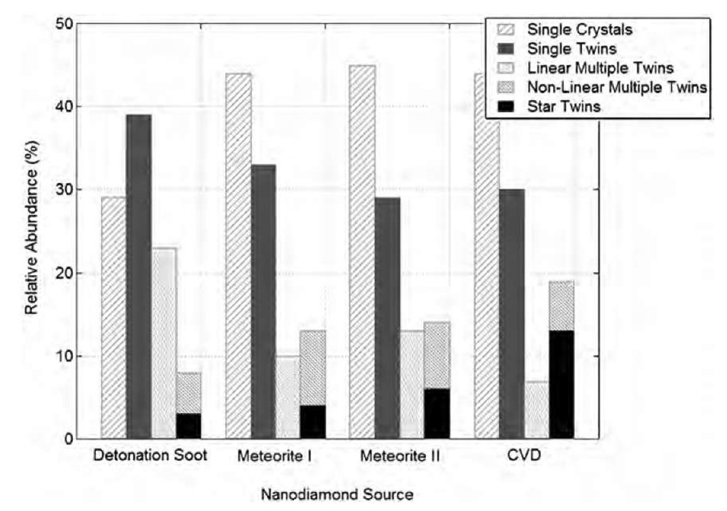
The crystallinity of nanodiamonds has been tested by diffraction, but is also directly observable by electron microscopy (enhanced atomic planes in Figs. 1 and 2 transmission electron micrographs). A complete crystal-lographic study of nanodiamonds produced in the three ways we have described (meteoritic, detonation, and CVD-UNC nanodiamonds) has been performed by Daul-ton et al.[8] in an attempt to determine the origin and synthesis mechanism of meteoritic diamonds. In all those types of nanodiamonds, twinning is often observed,preferentially for the largest particles. Twinning can take different forms, from simple twins, to multiple, to even fivefold star twins. However, the shape of the nanoparticles is globally spherical (Fig. 5).
Fig. 5 Distribution of different twinning types in nanodiamonds from various origins. The meteoritic diamond originated from the Murchison meteorite (I) and the Allende meteorite (II). One can note the similarity in the twinnings in meteoritic and CVD nano-diamonds.
The structure of the nanodiamond surface is little known. sp2-bonded carbon may be present at the surface and in UNC diamond film grain boundaries.[34] Hydrogen is present in all three varieties of nanodiamonds, but other impurities have been evidenced in detonation-produced and extraterrestrial nanodiamonds.
Maillard-Schaller et al.[35] have measured the impurity content of detonation-produced nanodiamonds by Raman and X-ray photoelectron spectroscopy (XPS). The major impurity is oxygen. The nitrogen content of their samples is 1-2% and traces of N, Fe, S, and Ar are also found. H2 plasma treatment of the nanodiamonds deposited on a Si substrate by electrophoresis causes oxygen impurities to leave the sample, whereas the nitrogen content remains the same. The sp3/sp2 content of the diamonds is unchanged by the high-temperature treatment.
NANODIAMOND PROPERTIES
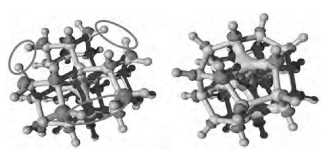
Very few theoretical studies of single nanodiamonds properties have been performed. Halicioglu[36] relaxed spherical nanometric diamond slabs with Brenner potentials. The so-formed structures exhibit inward relaxation from the top surface layers, the interatomic distance between neighboring atoms decreasing from the center of the cluster to the surface. They also noticed significant variations in relative cohesive energy with respect to bulk diamond. Recently, an ab initio molecular dynamics simulation, a parameter-free technique that solves quantum mechanical equations with great accuracy, was used to simulate the structure and to compute the electronic and optical properties of nanodiamonds.[23] Contrary to classical treatment, the quantum simulation of nanodia-monds yields an expansion of the cluster volume with respect to bulk diamonds. That tensile stress is at the opposite of what is observed in Si or Ge nanoparticles. The surface reconstruction of nanodiamonds has been shown to strongly affect electronic structure, as shown in Fig. 6.
Fig. 6 Structure of a 0.7-nm 29-carbon atom cluster. Left: The fully hydrogenated cluster. Right: The result of surface reconstruction induced by the removal of six pairs of hydrogen atoms (circled on the left). Carbon atoms are in light grey; hydrogen atoms are in dark grey. The isosurfaces represent the lowest unoccupied molecular orbital (LUMO; here located on the C—H bonds) and the highest occupied molecular orbital (HOMO; here located at the center of the cluster) drawn at 30% of their maximal value.
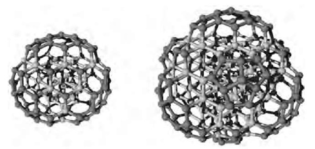
Fig. 7 C147 and C275 bucky diamonds. The diamond core atoms are represented in light grey.
When the totality of hydrogen is removed from the cluster, the surface is shown to sometime reconstruct in a specific way, forming the so-called ”bucky diamonds.” These structures consist of a diamond core the surface of which is reconstructed in a fullerene-like manner (Fig. 7).
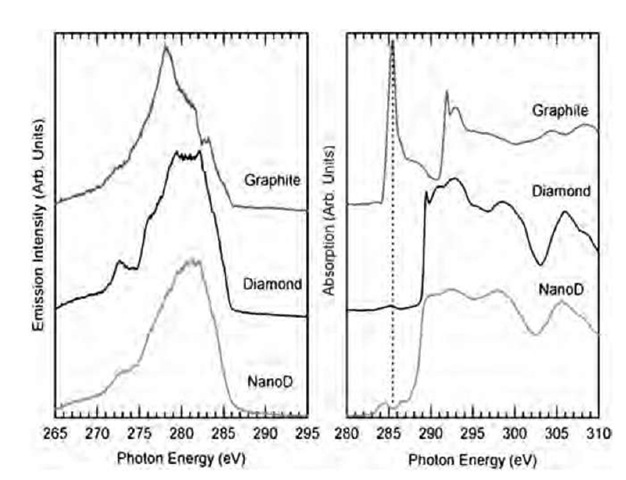
The optical properties of nanodiamonds have been studied mostly by X-ray techniques. The X-ray emission and absorption spectra of detonation nanodiamonds are very similar to those of bulk diamonds and are totally different from graphite (Fig. 8).
Fig. 8 X-ray emission (left) and absorption (right) spectra from highly oriented pyrolitic graphite (HOPG), bulk diamonds, and detonation-produced nanodiamonds (4 nm average size).
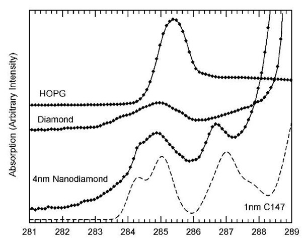
Fig. 9 Detail of the pre-edge X-ray absorption spectra of HOPG, bulk diamonds, and detonation nanodiamonds vs. the X-ray energy in electron volts. The density of unoccupied states computed ab initio from a C147 bucky diamond is shown for comparison (dashed line).
The differences between bulk diamonds and nanodia-monds are exciton broadening (289.3 eV) and a shallower secondary minimum (302 eV). However, there are some pre-edge features in the nanodiamond absorption spectrum that are not caused by impurities and are reproducible (Fig. 9). These features could be the signature of specific surface reconstructions such as in bucky diamonds.
Other information can be obtained from Fig. 8: There is no shift in valence and conduction band maximum and minimum in comparison with bulk diamonds. This indicates that quantum confinement does not affect the electronic structure for particles 4 nm and larger. This property can also be observed on computed absorption spectra from Fig. 10.
The optical properties of UDD layers have been studied optically and by XPS by Aleksenskii et al.[37] The band gap is measured to be 3.5 eV, with many energy levels present in the nanodiamonds band gap and contributing to a broad luminescence band (380-520 nm). The optical absorption of the material is attributed to threefold coordinated atoms on the surface. The unannealed sample contains 8% N and 22% O, mainly under the form of nitrate ions attached to the particle’s surface.
The electron transport in ultradisperse diamonds deposited on quartz substrates has been measured by He et al.[40] The conductivity of the films is shown to decrease with annealing. Surprisingly, it is semiconducting at high temperature but the temperature dependence of the conductivity is negative at lower temperatures. This behavior is attributed to conduction through surface conduction (p-type because of graphite-like sheets) at low temperature and through diamond core a-type conduction at higher temperature.
Fig. 10 Optical spectra of carbon clusters ranging from methane to 1-nm nanodiamonds. The spectra are computed using the time-dependent local density approximation on ab initio-relaxed cluster geometries. (From Refs. [38] and [39].) The dashed line shows the bulk absorption threshold computed with the same method (4.23 eV for an experimental value of 5.5 eV).
An interesting property of a hydrogenated diamond surface is its ”negative electron affinity,” the ability of an electron that is excited in the conduction band to freely leave the material. Nanodiamonds have smaller bandgaps than bulk diamond, and for that reason are excellent candidates for low-threshold electron emission devices. The additional requirement is that the electron affinity is small, or even negative. The electron emission of the UDD film from Ref. [40] is strong and has a low field threshold (3.2 V/p.m). It has been attributed to grain boundaries of nanodiamond films, rather than substrates. A similar field emission study was performed on ultrananocrystalline diamond films by Krauss et al.[41] The emission is again attributed to conduction through the grain boundaries-vacuum interface. With moderate heating (200-300°C), the photoemission yield is increased by a factor of 5.[42] When the hydrogenated UNC film is exposed to air, electron affinity is actually shown to become negative. A similar negative electron affinity has been measured after treating a film of deposited nanodia-monds obtained from detonation, but only after treating the film with H2 plasma, which removes most of the impurities, except nitrogen.[35]
NANODIAMOND NITROGEN N-DOPING
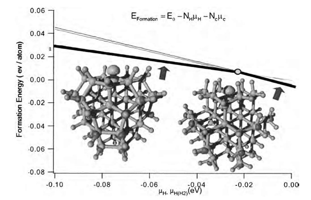
A very promising way to have nanodiamond films incorporated in technological applications is by doping them with nitrogen. The goal is to introduce carrier levels into the diamond gap (this level is located 1.7 eV below the conduction band minimum in bulk diamonds) to increase conductivity and to lower the electron emission voltage threshold. Nitrogen is a major impurity of natural diamond. As we said before, nanodiamonds produced by detonation contain a high percentage (12%) of nitrogen. This nitrogen is brought into the diamonds from the trinitrotoluene reactant and cannot be removed from the nanoparticles.[35] The precise location of the nitrogen atoms in the nanoparticles is uncertain, but several magnetic studies have been unable to see any trace of substitutional nitrogen (known as P1 center).[24] This is surprising as nitrogen is present in N-doped CVD-produced microcrystals as a substitute to core carbon atoms.[43] A theoretical study of the grain boundaries of UNC diamonds in the presence of nitrogen impurities has been performed by Zapol et al.[44] This tight-binding density functional study shows that nitrogen substitution to carbon in the grain boundary is energetically more favorable than in the crystal’s core. The conductivity increase of the N-doped film is then attributed to an increase in threefold coordinated carbon atoms caused by the nitrogen impurity. A recent ab initio molecular dynamics study[39] shows that for small diamond clusters, nitrogen is preferentially present as a substitute to surface carbon. The tensile stress evidenced in those nanoparticles[23] facilitates nitrogen inclusion in comparison to bulk diamonds, where intentional nitrogen doping has proven to be difficult. Nitrogen incorporation is shown to require more and more energy with increasing particle size (Fig. 11).
Fig. 11 Formation energy of 66 carbon atom clusters containing one nitrogen impurity atom as a function of the hydrogen chemical potential mH (eV). This energy is the difference between the cluster’s total energy and the energy the same number of carbon and hydrogen atoms (NC and NH) would have in their most stable form (here we consider diamond and the H2 molecule). The origin of mH (eV) is taken as the energy of one hydrogen atom in the H2 molecule. The thick black segments indicate the most stable structures. The stable configurations are the C65H65N and C65H39N clusters. In these, the nitrogen atom is substitutional in the particle’s surface. Above ~ — 0.02 eV, the stable structure is a fully hydrogenated cluster in which the nitrogen atom (in blue) sits on the surface. Below this energy (this would correspond to a higher temperature and/or a lower hydrogen pressure), the stable structure has a partially reconstructed surface in which the nitrogen resides. The C65H66N and C65H40N clusters in which the nitrogen atom is substitutional to a core carbon atom are never stable (thin lines). The isosurfaces are drawn at 30% of the maximal value of the HOMO (on the nitrogen atom) and LUMO (on C-H bonds), respectively.
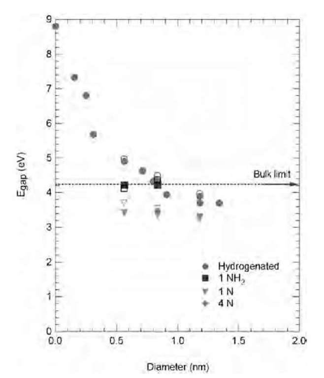
Nitrogen doping of UNC films has been studied by Bhattacharyya et al.[45] Doping is achieved by introducing nitrogen gas (1-20%) into the mixture fed to the CVD reactor. They achieved the highest carrier concentration and electrical conductivity ever measured for a phase-pure diamond thin film. The increase of N2 gas concentration causes larger grain boundaries and larger grains to be deposited, and increases the conductivity up to 143 1 cm-1 This large conductivity is attributed to the large proportion of nitrogen atoms in the grain boundaries. The optical and emission properties of N-doped UNC diamond films are still under investigation. A theoretical study[39] has compared the energy gap of hydrogen-terminated nanodiamonds clusters and clusters including various nitrogen impurities on the surface as a function of size. The variation is faster for reconstructed surfaces because of the size evolution of the surface curvature. For nonreconstructed surfaces, the curvature changes little with cluster size and the energy gap remains almost constant and smaller than for H-terminated clusters (Fig. 12).
NANODIAMONDS FOR THE FUTURE
Nanodiamonds are very promising materials for application, especially under the form of ultrananocrystalline diamond thin films. An extensive review of UNC film properties and potential applications can be found in Ref. [27]. We have cited the perspectives offered in field-induced and light-induced induced emission by nitrogen-doped UNC films. They could be used to produce bright, low-voltage (cold) cathodes. They may be used in the future as microelectromechanical system (MEMS) materials. Pioneer devices have been successfully produced by Krauss et al.[46] The exceptional hardness, fracture strength, and inertness of the films,together with a smooth surface, make UNC a unique material for miniaturized mechanical systems and devices, such as cantilevers, gears, etc. The hydrogen termination of the surface also brings a ”natural lubricant” to the moving devices.
Fig. 12 Computed HOMO-LUMO energy gaps for various nanodiamonds structures. Red circles: Hydrogenated nanoclus-ters; black squares: nanodiamonds with a NH2 surface group; green triangle: one surface substitutional nitrogen; pink diamond: four surface substitutional nitrogen atoms. The filled symbols represent the nonreconstructed, maximally hydrogenated nano-diamonds; the empty symbols represent (100) reconstructed surfaces.
UNC diamonds also have potential applications in optoelectronics, as photonic switches, electronic devices (pn junctions), etc. They are on their way to being commercially used as surface acoustic wave devices. Recent experiments have even used UNC films as support to attach ADN.[47] These devices have proven to be extremely stable and have opened the way to the integration of biology in electronics.
CONCLUSION
Nanodiamonds have unique, fascinating properties, as isolated particles or in thin films, but many aspects still have to be understood. The interaction between nanodia-monds is largely unknown. The most intriguing fact is that all types of nanodiamonds have similar features and size distributions (independently of the production type), extreme pressure and temperature, and low-pressure CVD, and are around stars. Indeed, everywhere where scientists have looked for carbon nanostructures with a high-resolution microscope, they found nanodiamonds. Would they not be everywhere around us?
![Optical spectra of carbon clusters ranging from methane to 1-nm nanodiamonds. The spectra are computed using the time-dependent local density approximation on ab initio-relaxed cluster geometries. (From Refs. [38] and [39].) The dashed line shows the bulk absorption threshold computed with the same method (4.23 eV for an experimental value of 5.5 eV). Optical spectra of carbon clusters ranging from methane to 1-nm nanodiamonds. The spectra are computed using the time-dependent local density approximation on ab initio-relaxed cluster geometries. (From Refs. [38] and [39].) The dashed line shows the bulk absorption threshold computed with the same method (4.23 eV for an experimental value of 5.5 eV).](http://what-when-how.com/wp-content/uploads/2011/03/tmp28C255_thumb_thumb.jpg)
