Direct Deposition of Porous Alumina on a Substrate
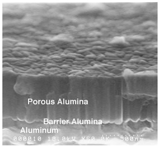
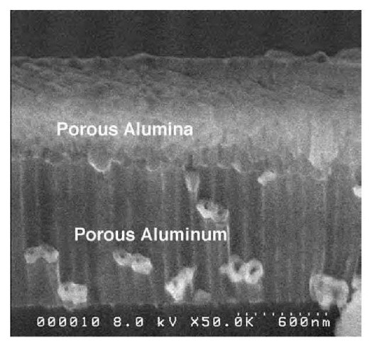
In our laboratory, we have recently demonstrated a novel method to deposit nanoporous alumina template on a substrate.[29] The method also allows transfer of the nano-porous template pattern onto the bottom substrate. The technique combines anodization process to produce template arrays and plasma etching through the pores. The sequence of steps is shown schematically in Fig. 9. We used silicon wafers as the starting substrate material, although in principle, the method can be extended to any other substrate, for example, epitaxial GaN.[30] A 5-nm-thick adhesion layer of Ti is deposited onto Si substrate by e-beam evaporation followed by a 1-mm-thick layer of Al. Without the Ti layer, the subsequently deposited nanoporous alumina membrane is found to peel from the Si substrate. The aluminum film is anodized in an acid under d.c. conditions for 2-3 min. A cross-section SEM image of the as-deposited template is shown in Fig. 10. The remaining Al layer following anodization and the alumina layer produced by the anodization process are clearly seen. The presence of a thin barrier layer of alumina (U-shaped barrier) is also seen at the pore bottoms. The thickness of the barrier layer in this case is only of the order of 10-20 nm. One major problem for applications based on this method is posed by etching of this barrier layer to pattern layers directly below. Wet chemical etching methods, such as dilute phosphoric acid, although attempted in the past by other research groups,[31,32] are not particularly useful. In addition to removing the barrier layer, it also causes pore widening,thus increasing pore diameter and, in some cases, completely removing the alumina film. We have used plasma etching to anisotropically remove the barrier layer without changing pore diameter. Plasma etching was carried out using a commercial inductively coupled plasma system with reactive ion etching (RIE). Cl2 diluted with Ar was used as etchant. The etch process required critical control over various parameters, in particular, etch power and etch time. Details of the process are described in Ref. [29]. Cross-section image of the final product after a 60-sec etch at 200-W RIE power is shown in Fig. 11. The pores in the top nanoporous alumina layer can be clearly seen. In addition, the etch has penetrated through the barrier region and continued down through the Al to the Ti adhesion layer. Some of the Al nanotubes produced by the process have snapped in cleaving, showing the hexagonal shape of the parent hole template. Following breakthrough of the barrier layer, etch time can be varied to control the depth of the aluminum pores. In fact, with the appropriate etchant, the etch can even be continued through the Ti layer into the bottom substrate. In this manner, a nanoporous pattern, which mirrors the pattern on the initial nanoporous alumina template, can be created on any substrate. The top nanoporous alumina layer can easily be removed by soaking in a mixed solution of 0.2 M chromic/0.4 M phosphoric acid. Fig. 12 shows an AFM image of the top view of the aluminum template postremoval of the porous alumina layer. The pore diameter is of the order of 50-60 nm similar to that of the initial alumina film. In the final stage, nanoarrays of various materials can be synthesized by depositing/growing them inside the pores.
Fig. 10 Left: SEM cross-section image before plasma etch showing nanoporous alumina layer at the top, barrier layer followed by aluminum layer below.
Fig. 11 Right: Cross-section image postplasma etch showing porous alumina layer and the porous aluminum layer below.
SELF-ASSEMBLED NANOARRAYS
Using the various methods discussed, nanoarrays of different materials have been successfully deposited. These include magnetic materials, semiconductor compounds, superconductors, and carbon nanotubes. A brief description of the properties of these nanoarrays is given below.
Magnetic Nanoarrays
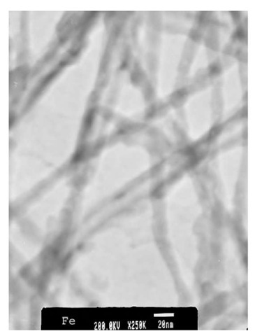
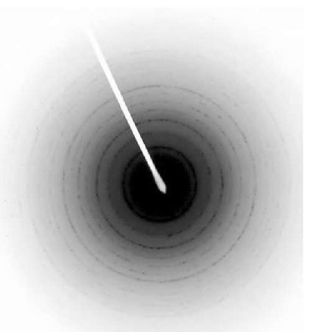
Current magnetic recording media are based on magnetic thin films where the information is stored on grains. To increase data storage density in such media, one must either reduce the size of the grains or reduce the number of grains that constitute each bit. Reducing the number of grains leads to increased noise and decreased size of grains leads to superparamagnetism where thermal energies alone are enough to flip the magnetization direction. These limits depend mainly on the anisotropy constant of the material and the aspect ratio of the grains. For present-day magnetic media, the superparamagnetic limit will be reached at densities of about 100 Gb/in2. Patterned media consisting of isolated single-domain islands where each island stores one bit of information are expected to overcome the above problem. It is thought that for such patterned media (with anisotropy constant equal to that of present-day magnetic media), storage densities as high as 1 Tb/in2 will be achievable. For such large densities, the size of the islands will have to be around 10 nm. Using porous alumina, one can easily fabricate nanomagnetic islands with feature size down to 10 nm. Materials such as Fe, Co, and Ni electrodeposited into the nanopores serve as a model system for the study of magnetic properties, interactions, and thermal stability of nanometer-sized particles. Several research groups have carried out investigations on the magnetic properties of Fe, Co, and Ni nanowires electrodeposited in porous alumi-na.[33-37] The standard synthesis procedure has been to use a.c. electrodeposition. The wires are in the form of cylinders positioned perpendicular to the film plane in a regular array. The wires have been characterized using electron diffraction measurements. Fig. 13 shows a TEM image of Fe nanowires released from alumina template and dispersed onto a substrate. The wire diameter is of the order of 10 nm. High-resolution TEM images of the wires reveal that the wires are polycrystalline in nature with grain sizes ranging from ~ 5 to 50 nm. Electron diffraction image for Fe nanowires is also shown in Fig. 14. Analysis of the image confirms a bcc crystal structure for these nanowires. Similar studies for Co and Ni nanowires reveal an hcp structure for Co and fcc structure for Ni [38,39] nanowires.
Fig. 12 Top view AFM image showing pores on aluminum layer.
Fig. 13 Transmission electron microscopic image of Fe nanowires released from porous alumina.
Fig. 14 Electron diffraction image of Fe nanowires.
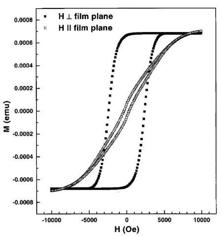
Magnetic properties of these nanowires exhibit strong perpendicular anisotropy. Fig. 15 shows a typical magnetization vs. field image for an array of Fe nanowires electrodeposited inside porous alumina. The diameter of the wires is around 10 nm, and the length is of the order of 1 mm. In the direction perpendicular to the film plane, the coercivity is very high, about 2341 Oe (remanence ratio 0.96), and in the parallel orientation, the coercivity is only about 300 Oe (remanence ratio 0.055). The nanowires thus possess uniaxial anisotropy with easy axis perpendicular to the film plane. The large anisotropy arises mostly from shape anisotropy because of the cylindrical shape of the nanowires. For a cylinder-shaped entity, the demagnetizing factor for field parallel and perpendicular to the cylinder axis are 0 and 2p, respectively. The shape anisotropy therefore forces the magnetization to be in the axial direction and is given by 2pMs, where Ms is the saturation magnetization. The anisotropy field can be estimated by extrapolating the magnetization curves using the Ms values for bulk Fe (1710 emu/cm3) and is estimated to be of the order of 8 kOe for Fe nanowires. These may be compared with theoretically predicted shape anisotropy field of 2pMs 10.7 kOe for Fe nanowires) for an infinite cylinder. The large perpendicular coercivity suggests resistance to magnetization reversal. The large perpendicular squareness in comparison to the parallel squareness indicates large remanent magnetization. All of these factors, large perpendicular squareness, high remanence, and the large coercivities, may make these materials useful for magnetic recording media.[40,41] For such applications, it is necessary to investigate the dependence of magnetic properties on size of the nanostructure.
Fig. 15 Magnetization vs. field for an array of Fe nanowires in the perpendicular and parallel direction.
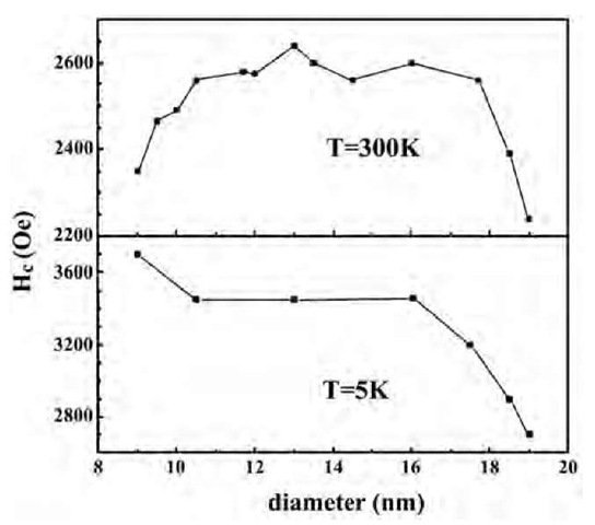
Fig. 16 Coercivity as a function of wire diameter for Fe nanoarrays, at room temperature and at 5 K.
We have carried out a systematic investigation of the magnetic properties of Fe nanowires as a function of length and diameter of nanowires.[42] For large length of the nanowires, of the order of microns, the coercivity Hc was found to be somewhat independent of length for fixed wire diameter. The coercivity, however, depends critically on the diameter of the wires. In general, the coercivity is found to decrease with increasing wire diameter. For example, Fe nanowires of diameter 32 nm exhibit a coercivity of ~ 2158 Oe which is about 200 Oe smaller than that for wires of diameter 9 nm. The decrease in coercivity is a result of development of multidomain structure in larger nanowires.
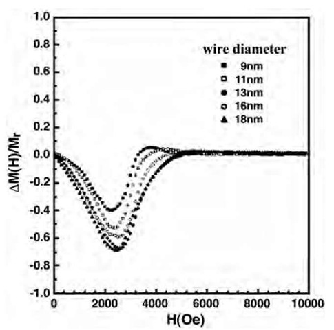
An interesting feature is observed for wires with very small diameter, <13 nm. As seen in Fig. 16, for diameter <13 nm, the coercivity is found to decrease. The maximum in coercivity therefore occurs at a wire diameter of about 13 nm and has a value of about 2640 Oe. In contrast to the behavior at 300 K, at 5 K, the coercivity exhibits a maximum for the smallest wire diameter investigated, namely, 9 nm (Fig. 16). The coercivity is around 3700 Oe at 5 K. Unlike the behavior at 300 K, for increasing wire diameter, the coercivity continually decreases. The nonmonotonic behavior at 300 K, in contrast to that at 5 K,can be explained as follows. At such small sizes, the wire diameter is much smaller than a single domain. Ferromagnetic domains cannot form and superparamagnetism dominates. Accordingly, the coercivity is low. Indeed, Li and Metzger[43] reported very small activation volumes, ~ 1.0 x 10"18 cm3, for small diameter Fe nanowires at room temperature. This value is very close to the theoretical superparamagnetic limit.[44] The superpara-magnetic effect will contribute to magnetization at low temperature below blocking temperature leading to the increase of coercivity at 5 K. Magnetic interaction between the wires is an important factor in recording media and can be estimated by measuring the quantity defined as DM.
where Ir(H) is d.c. demagnetization remanence and Ir(H) is isothermal remanence. For isothermal remanent magnetization measurements, the sample was first demagnetized. A magnetic field was then applied and reset to zero and the remanent magnetization was measured. This was carried out for different field values, and the isothermal remanent magnetization curve was obtained as a function of the field. In the case of the d.c. demagnetization curve, the sample was first saturated in a high field of 13 kOe and the remanent magnetization was obtained at various values of the reversal field. Fig. 17 shows the DM plots for Fe wires with different diameters. All of them show negative peaks, suggesting presence of magnetostatic interaction.
Fig. 17 DM plots for Fe nanowires of varying diameter.
Magnetic properties of Co and Ni nanoarrays electro-deposited in porous alumina have also been studied in great detail by various authors. The largest coercivities for Ni nanowires have been reported by Nielsch et al.[36] They obtained coercivity of ~ 1200 Oe for highly ordered Ni wires of diameter 30 nm with remanence of the order of 100%. The diameter of the wires was varied in the range 30 to 55 nm while keeping the nanowire distance constant (100 nm) and found that the coercivity drops to 600 Oe (remanence ~ 30%) for wires of diameter 55 nm. Magnetic measurements for Co nanowires in anodic alumina templates have been studied extensively by Zeng et al.[45] For a fixed wire diameter of about 10 nm, as the nanowire length is increased, Hc is found to increase steeply until a constant value of about 2300 Oe is approached at wire lengths of about 200 nm. For larger wire lengths, the coercivity is more or less independent of length. For wire lengths of the order of 500-1000 nm, the coercivity is found to decrease gradually with increasing nanowire diameter. This is accompanied by shearing of the hysteresis loop. Both the decrease of Hc and the shearing of the loop are attributed to magnetostatic interactions.
Time dependence of magnetic properties of Fe, Co, and Ni nanoarrays has been studied.[46-48] Quantities such as magnetic viscosity and activation volume have been calculated, and models for reversal mechanism in these nanowires have been extensively investigated. Typically, the activation volume for wires with diameter of the order of 10 nm is calculated to be of the order of ~ 4 x 10"18 cm3. This value is much smaller than the physical wire volumes, which indicates that magnetization reversal starts in a small region of wires. Magnetic reversal mechanisms such as coherent rotation and curling treat the wires as perfect homogeneous cylinders. However, the coherent rotation and curling modes are delocal-ized and could lead to activation volumes much larger than those observed. A more reasonable explanation of the reduced coercivities and thermal activation volumes encountered in electrodeposited nanowires is morphological inhomogeneities. Transmission electron microscopic results indicate a considerable degree of polycrystallinity with crystallite diameter of about 5 nm. Polycrystalline wires can be interpreted as random-anisotropy ferromag-nets where interatomic exchange tries to align the local spins, but the exchange stiffness has to compete against random-anisotropy forces associated with the local uniax-ial anisotropy. As a consequence, the magnetization processes become localized.[49] The localization length or physical activation volume strongly depends on crystallite size.
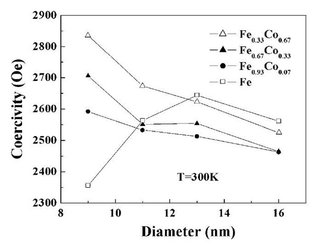
As discussed earlier, in nanowires, magnetic anisotropy originates mainly from shape anisotropy. Large-shaped anisotropies can result from large saturation magnetization, which, in turn, can lead to large coercivity. This suggests that large coercivities are expected in FeCo nanowires because in bulk form, these alloys exhibit large saturation magnetization (1950 emu/cm3 for 35 at.% Co) which is larger than both Fe and Co. We have successfully electrodeposited FeCo alloys into the pores.[50] For these arrays, we did observe coercivity for some FeCo nano-wires to be larger than that of Fe and Co. The coercivity is found to be 2600 Oe for Fe0.93Co0.07, 2900 Oe for Fe0.67Co0.33, 2850 Oe for Fe0.33Co0.67, and 2400 Oe for Fe0.07Co0.93. The coercivity is largest for Fe0.33Co0.67 and Fe0.67Co0.33 samples and is much higher than those obtained for Fe (2400 Oe) and Co (1900 Oe) prepared under similar conditions. As in the case of elemental Fe, Co, and Ni nanoarrays, we obtained very high squareness ratio 1) for most of the samples, suggesting excellent perpendicular magnetization characteristics. Fig. 18 shows the variation of coercivity as a function of diameter of the nanowires for all the Fej -xCox alloys. Length of the nanowires is kept constant in all the samples 3 mm). It is noted that contrary to the behavior of pure Fe, Fe-Co alloys show no maximum in coercivity as a function of wire diameter, suggesting that the superparamagnetic behavior is eliminated even for the smallest diameter wires (9 nm) used in this study. With increasing Co addition, the saturation magnetization and hence shape anisotropy constant of Fe-Co alloys are increased, which should result in higher energy barrier E (given by KV, where K is the anisotropy constant and V is the volume).
Fig. 18 Variation of coercivity as a function of wire diameter for FeCo alloys.
Semiconductor Nanoarrays
Alternating current or direct current electrodeposition can be used to fabricate arrays of semiconducting nanowires/ nanodots in porous alumina. Electrochemically, the most easily fabricated semiconductors are the II-VI semiconductors of the type CdS, CdSe, etc. This can be achieved using three different methods. In the first method used by Moskovits,[51] a metal capable of forming a semiconductor is first electrodeposited into the pores of alumina. The top surface of the porous aluminum oxide is then etched away in an acid to expose the ends of the metallic array of wires. The deposited metal is then allowed to react with a liquid or gaseous reagent to convert them chemically to a semiconductor. For example, cadmium particles can be converted to CdS by reaction with sulfur vapor or hydrogen sulfide. Gallium particles may be converted to GaAs by reaction with arsine.
In the second method, sulfuric acid is a.c.-electrolyzed causing the sulfide atoms to be deposited in the pores. This is followed by a.c. electrodeposition of Cd into the pores, allowing the S atoms to react chemically with the Cd atoms, causing formation of CdS. Instead of a.c. electrodeposition of Cd, one may simply soak the porous template containing S atoms into a boiling solution of cadmium sulfate.
In the third method, the electrolyte used for the electrodeposition is nonaqueous unlike that used for magnetic materials.[52,53] For the preparation of semiconductor nanowires of MX (M = Cd, Pb, Zn and X = S, Se, Te), a solution of dimethylsulfoxide containing a salt of M (50 mM) and elemental X (S or Se) is used. For example, CdS is electrodeposited using a 50-mM solution of cadmium perchlorate and 50 mM S in a dimethyl-sulfate solution. A small amount of lithium perchlorate is also added to improve the conductivity.
We have successfully prepared nanowires of CdS, CdSe, PbSe, ZnSe, etc. using the deposition methods described above. Details of our studies on these nanoar-rays and their possible device applications are discussed in detail in Ref. [54]. Such nanowire arrays can be used to study their electrical properties and thus investigate their potential applications in devices such as diodes, transistors, photodetectors, and light-emitting devices. Semiconductor nanodots and nanowire devices could be the building blocks for digital nanoelectronics, an integrated circuit technology which will permit downscaling to be carried beyond what is currently achievable.
Energetic Nanocomposite Nanoarrays
Energetic materials are a class of substances consisting of an appropriate mixture of a fuel and oxidizer material. When ignited, they release a large amount of energy because of an exothermic reaction. Such materials have several applications, in explosives, propellants, etc. Recently, it has been found that when fabricated in the form of nanocomposites, the energetic properties are highly enhanced.[55]
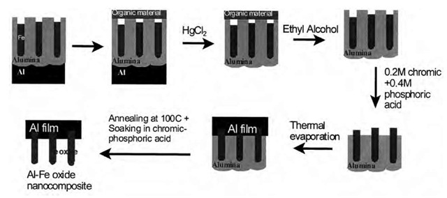
Using porous alumina templates, we have developed two novel methods to fabricate these materials. In both methods, a thin film of Al is the fuel material and Fe oxide nanowires are the oxidizer material. Al film is prepared by means of thermal evaporation, while the nanowires are prepared by means of electrodeposition inside nano-porous alumina templates. We have found that presence of aluminum oxide around the wires inhibits direct interaction between Al and iron oxide. The aluminum oxide barrier layer and the aluminum oxide around the wires therefore need to be completely removed. Fig. 19 shows the sequence of steps that we followed to achieve this.[56]
Fig. 19 Sequence of steps to prepare Al-Fe oxide nanocomposites (method 1).
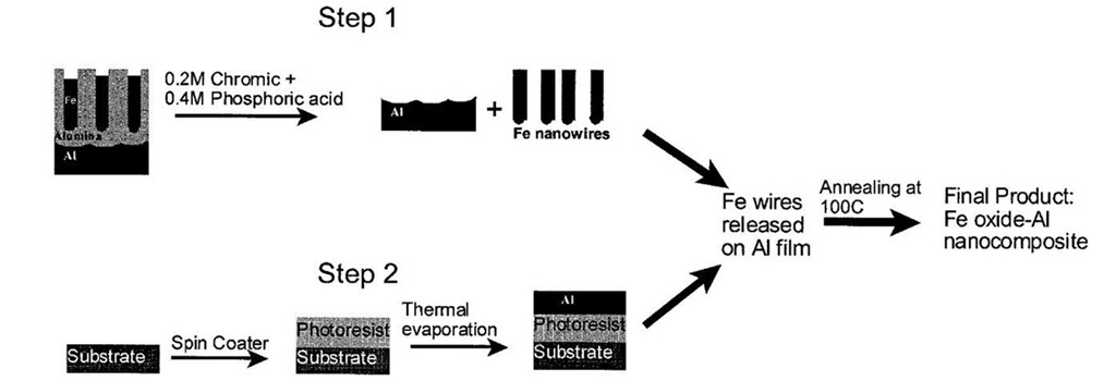
The electrodeposited sample is first coated with a thin organic layer. The sample is then soaked in 3% mercuric chloride solution, which removes the bottom Al layer. The top organic layer protects Fe wires inside the pores from being etched away by mercuric chloride solution. In the next step, the organic layer is removed in ethyl alcohol solution and the sample is dried. The sample is now soaked in a mixture of chronic-phosphoric acid at 60°C to partially etch the pores from the top revealing Fe wires. The sample is rinsed and dried, and a thin film of Al (50 nm) is coated on top by means of thermal evaporation. Al film is therefore in contact with the Fe nanowires. The sample is annealed at 100°C for a few minutes to improve the interface contact between Al and the Fe nanowires. It is then soaked in chromic-phosphoric acid mixture to etch away the remaining aluminum oxide film. This leaves behind an Al film attached to an array of Fe nanowires. The sample is cleaned, dried, and annealed to completely remove trace amounts of water vapor and also to convert Fe nanowires into Fe oxide. In method 2 (see Fig. 20 for sequence of steps), a thin film of photoresist material is deposited on a glass wafer followed by thermal evaporation of a thin layer of aluminum (50-nm thickness). A commercial Al foil is anodized separately under d.c. conditions at 40 V in 3% oxalic acid for 30 min, creating a nanoporous template with pore diameter of the order of 50 nm. Fe nanowires are electrodeposited inside the pores under a.c. conditions. The sample is then soaked in a mixed solution of 0.2 M chromic/0.4 M phosphoric acid at 60°C. The acid mixture dissolves aluminum oxide completely leaving behind the Fe wires in solution. This solution is poured onto the thermally evaporated Al film. The Al film is annealed at 100°C to improve adhesion of Fe nanowires, followed by rinsing and drying to remove traces of the acid. The sample is then soaked in a solution of acetone to dissolve the photoresist material. This leaves behind the final product, Al-Fe oxide nanocomposite film, which is rinsed in methanol followed by annealing at 100°C for a few minutes to remove all traces of water vapor. Al-Fe oxide nanocomposite prepared using these two methods is found to ignite readily under flame ignition, indicating several possible applications of these materials in explosives, propellants, and other military applications.
Carbon Nanotube Arrays
Carbon nanotubes[57] can be viewed as rolled-up sheets of graphite with diameters approximately a few nanometers. They can be either metallic or semiconducting, with band gaps that can be controlled by controlling the tube diameter. Several applications are envisioned for these materials. Carbon nanotube electronics are expected to provide a viable alternative to silicon when chip feature sizes cannot be made any smaller using silicon.[58] Nano-tube electronics are also expected to provide great progress in computer miniaturization and computing power. They have potential applications in cold-cathode flat panel displays because of their excellent field emission properties.[59] Carbon nanotubes can be used to encapsulate other materials such as Fe, Co, etc.[60] They can be used in infrared imaging, inert membranes for biomedi-cine, etc. They can be placed on an Scanning Probe Microscopy (SPM) tip to manipulate molecules with sub-angstrom accuracy.[61] The tips are atomically precise with chemistry similar to C60, and thus serve as functional elements with a wide variety of molecular fragments. Functionalizing carbon nanotube tips will allow mechanical manipulation of many molecular systems on various surfaces with sub-angstrom accuracy.
For several of the applications described above, particularly in nanotube electronics, it is necessary to be able to control the growth of carbon nanotubes both with respect to size and orientation. Carbon nanotube arrays have been successfully synthesized in ordered porous alumina templates.[62-66] The diameter and spacing of the carbon nanotubes are controlled by controlling the diameter and interpore spacing in porous alumina. Most of the methods involve initial deposition of Co inside the pores which act as catalyst for the growth of carbon nanotubes. Earliest demonstration of carbon nanotube synthesis in porous alumina was provided by Li et al.[65,66] A small amount of Co is electrodeposited in the pores, and the templates are heated in a tube furnace at 600°C for 4-5 hr under CO flow (100 cm3/min). The CO flow is then replaced by a mixture of 10% acetylene in nitrogen at a flow rate of 100 cm3/min for about 2 hr at 650°C. The samples are then annealed for 15 hr in nitrogen leading to formation of an array of carbon nanotubes. The carbon nanotubes produced in porous alumina templates have the following common characteristic features: they always grow perpendicular to film plane, are multiwalled, have uniform sizes, and are open-ended. The growth of carbon nanotubes inside pores by catalytic decomposition of organic vapors has been postulated as either base or tip growth.[67] Scanning electron microscopic studies indicate residual Co/Fe catalyst in the base of the tubes, indicating that a tip growth mechanism could be responsible for the tube growth. It is also thought that the surrounding alumina may also be acting as a catalyst in nanotube growth.[68]
Fig. 20 Sequence of steps to prepare Al-Fe oxide nanocomposite (method 2).
Field emission characteristics of ordered carbon nano-tubes have been investigated.1-63-69-1 Yuan et al.[63] demonstrated excellent field emission characteristics for these nanotube arrays. In their measurements, they removed the barrier layer between the aluminum and the porous layer. Field emission was seen to begin at a relatively low electric field 2.8 V/m). They measured a very large emission current 0.08 mA/cm2 at 3.6 V/mm, much greater than that reported by Davydov et al.[69] for as-prepared nanotube arrays (in presence of barrier layer). Over a period of 150 hr, no significant reduction in emission current was observed. In contrast, in the presence of the barrier layer, the current density was found to decrease rapidly with time over a period of a few minutes. Another reason for the enhanced field emission may be related to the open-ended nature of the carbon nanotubes, which results in smaller radius of curvature than the closed ends, thus causing electrons to be emitted more easily. In a similar study, Jeong et al.[70] measured a turn-on field of 1.9-2.1 V/mm and a field enhancement factor of 33605200. In their samples, the barrier layer is absent and the density of carbon nanotubes was very small, ~ 107 tips/ cm2. The intertube distance is therefore higher, minimizing field screening effect and, in turn, enhancing field emission effect.[71] Field emitter arrays with such high emitting efficiency are expected to have applications in flat panel displays in the near future. For application in nanoelectronics, it is sometimes necessary to be able to make connections between carbon nanotubes. One solution is to directly prepare T- or Y-junction carbon nanotubes. In general, pores inside nanoporous alumina are straight when the anodization voltage is kept fixed during anodization. However, one can create branched pores inside alumina by changing the anodization voltage during anodization. In particular, Y-shaped pore forms in porous alumina when the anodization voltage is reduced by a factor of 1/ 2 during the anodization. Li et al.[66] synthesized Y-junction carbon nanotubes in such templates by using Co as a catalyst and by pyrolysis of acetylene at 650°C. Papadopoulos et al.[72] obtained electronic transport measurements on both individual and parallel arrays of Y-junction nanotubes synthesized in porous alumina. Nonlinear transport and rectifying behavior was observed. This behavior can be explained in terms of a change in band gap across the junction caused by the change in diameter across the junction. Y-junction carbon nanotubes are thus a realization of semiconductor heterostructures in the nanometer scale. Y-shaped nano-tubes and nanowires are expected to have possible applications in room-temperature single electron transistor and spintronic devices.
CONCLUSION
In conclusion, porous alumina is indeed a versatile template. It allows fabrications of a variety of nano-structures in the form of nanoarrays with feature sizes as small as 10 nm. As described in this article, characterization and measurement of appropriate properties of the nanoarrays can be easily carried out. It allows investigation of several fundamental phenomena at the nano-scale level and also allows for investigation of potential applications of nanostructures in future high-performance nanoscale devices.
