Molecular-Assembly Nanowires on Mica Surface
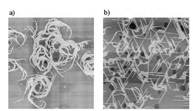
Fig. 7 shows the surface morphologies of the CT complex of (1)(F4-TCNQ)2 that transferred onto freshly cleaved mica by a single withdrawal from monolayer on a) pure water and b) 0.01 M KCl subphase. Although both films showed the formation of molecular-assembly nanowires, significant difference about the nanowire orientation was confirmed between them. Both nanowires had typical width of 50 nm and height of ~ 2.5 nm. By introducing 0.01 M KCl into the subphase, the nanowire orientation appeared as network structure connecting the well-developed nanowires to each other. Almost all the nanowires on the mica surface formed an angle of 60° to each other.
Fig. 7 Surface morphology of transferred nanowires of (1)(F4-TCNQ)2 from a) pure water and b) 0.01 M KCl. The scales of AFM images are 10 x 10 mm2.
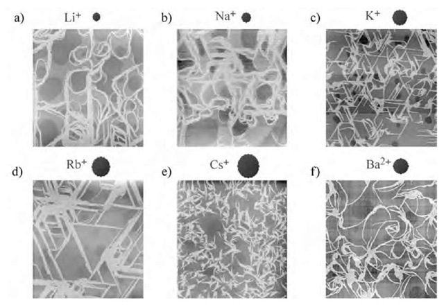
Fig. 8 Surface morphology of transferred nanowires of (1)(F4-TCNQ)2 on mica from a) LiCl, b) NaCl, c) KCl, d) RbCl, e) CsCl, and f) BaCl2 containing subphase. The concentration of ions in the subphase was fixed at 0.01 M. The scales of AFM images are 10 x 10 mm2.
Because the F-A isotherm of (1)(F4-TCNQ)2 between pure water and 0.01 M KCl subphase was almost consistent with each other, the CT complex may not recognize K+ ion at the air-water interface. Therefore the orientation of nanowire should occur during the film deposition processes because the orientation direction of the nanowires was consistent with the crystal lattice of mica.[33,34] The morphology of nanowires on mica surface strongly depended on the cation species that were introduced into the subphase (Fig. 8). When we introduced Li+ (ion radius rj=0.6 A) or Na+ (rj=0.95 A) into the subphase, although the formation of nanowires were confirmed, the nanowire orientation completely disappeared. Much larger cation of Cs+ (rj=1.69 A) yielded the ill-developed molecular nanowires with maximum length of less than ~ 1 mm. In the case of Rb+ (rj=1.48 A), well-developed oriented nanowires were observed at a typical length of above 2 mm. The most densely developed oriented nanowires were confirmed by the introduction of K+ (rj= 1.33 A) into the subphase, which resulted in a typical nanowire dimension of 2.5 x 50 x-2000 nm3. Although Ba2+ (r,= 1.35 A) has almost similar ionic radius to that of K+, the nanowire orientation completely disappeared on the mica surface.
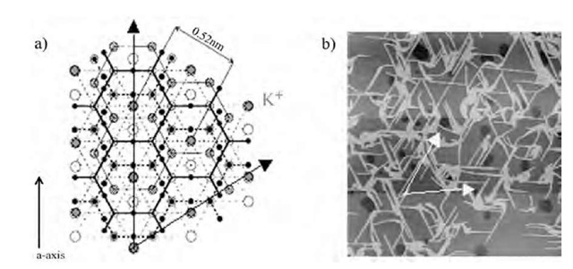
Fig. 9 a) Crystal structure of mica surface. Hexagonal arrays of K+ sites are indicated by red closed circles. b) Atomic force microscopy (AFM) image of oriented nanowires on mica surface deposited from 0.01 M KCl subphase. The white allows correspond to hexagonal lattice of K+ site on mica, showing the relation between the nanowire orientation and K+ array.
The difference of the nanowire orientation according to the ions is related with the surface property of mica rather than the ion radius. Mica has a typical composition of KAl3Si3O10(OH)2, and vacant potassium sites of sixfold symmetry appear by the cleavage (Fig. 9).[33,34] These K+ sites should be negatively charged and attract cations when the mica substrates are immersed in the K+-containing subphase. The nanowire orientation may occur by matching of the surface potential of mica surface and that of the nanowires, rather than by ion recognition of individual molecules. The anionic species of F4-TCNQ anion radical should be embedded on K+, and nanowires may orient in an epitaxial way through the lattice matching between mica and nanowires. Such recognition mechanism is the most probable explanation for the nanowire orientation. Although the dimension of nano-wires is much larger than the unit cell of hexagonal array of K+ on mica surface, the nanowire orientation was affected by the K+ array on mica surface.
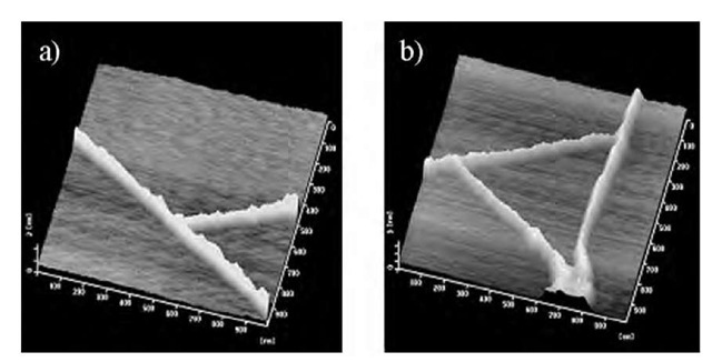
Fig. 10 shows selected AFM images (1 x 1 mm2) of oriented molecular-assembly nanowires on mica. As previously mentioned, the nanowires oriented 60° to each other, which provided interesting nanoscale structures such as nanowire tree and triangles. The six-folded connecting modes of each nanowire form novel nanoscale junction structures, which can apply for constructing the integrated nanoscale electronic circuits.
Molecular-Assembly Structures Within Nanowire
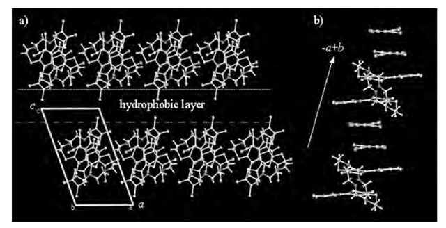
The single crystal of (2)(F4-TCNQ)2 were obtained, and here donor 2 is the four-alkyl chain derivative of compound 1. Assuming a similar molecular packing structure of CT complex between (2)(F4-TCNQ)2 and (1)(F4-TCNQ)2, we can discuss the molecular-assembly structure in the nanowires based on the crystal structure of (2)(F4-TCNQ)2.[35] Fig. 11 shows the unit cell of (2)(F4-TCNQ)2 viewed along the b axis. Donor 2 formed an intramolecular p-p dimer through folding of the flexible 24-crown-8 moiety, in which the p-planes of the two TTF units overlapped at their inner C3S5 rings. Along the c axis, the D-A layers are separated by the hydrophobic decylthio chains; moreover, the hydrophilic and hydrophobic layers are alternately arranged. The crystal structure suggests that the direction normal to the substrate surface in the LB film is consistent with the c axis (c = 1.72 nm). As indicated in Fig. 11, which shows the p-p stacking structure within the ab plane, the p-p dimer structure of F4-TCNQ stacked alternately with the intramolecular TTF dimer along the —a + b axis. The p-p stacking sequence between donor 2 and F4-TCNQ was -D-A-A-D-, forming a 1-D mixed-stack structure.
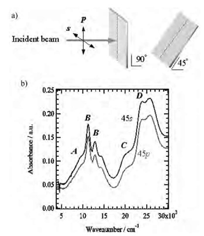
The molecular orientation within the LB films was evaluated by using the polarized ultraviolet-visible-near infrared (UV-vis-NIR) spectra.[19-21] The polarized UV-vis-NIR spectra of the LB film of (1)(F4-TCNQ)2 did not indicate any in-plane anisotropy with the normal incidence, indicating the isotropic distribution of molecular orientation within the substrate surface. Two sharp absorptions (B bands) were assigned to the intramolecular transition of the F4-TCNQ— anion radical,[36] while the C and D bands were assigned to the intramolecular transitions of TTF+ and F4-TCNQ—, respectively.[37] The broad A bands were assigned to the intramolecular transition of bis(TTF)-macrocycles,[38-40] which overlapped with the B bands. With 45° incidences (Fig. 12a), the absorption intensity for the s-polarization was larger than that for the p-polarization. Because the intramolecular transition moments of donor 1 and F4-TCNQ lie along the long axes of TTF and F4-TCNQ molecules, the long axes of donor 1 and F4-TCNQ were relatively parallel to the substrate surface.
Fig. 10 Selected AFM images of oriented molecular-assembly nanowires. a) Nanowire tree and b) nanowire triangles. Scale of AFM images are 1 x 1 mm2.
Fig. 11 Crystal structure of CT complex (2)(F4-TCNQ)2. a) Unit cell viewed along the b axis. b) Alternate p-p stacking structure between donor 2 and F4-TCNQ dimer along the — a+b axis. Alkyl chains are omitted.
Fig. 12 Polarized UV-vis-NIR spectra of the LB film of (1)(F4-TCNQ)3. a) Optical arrangements of the substrates to measure the polarized UV-vis-NIR spectra at 90° and 45° incidence. b) Polarized UV-vis-NIR spectra of 45° incidence with p- and s-polarization.
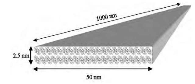
From the results of X-ray structural analysis and polarized UV-vis-NIR spectra, we constructed the schematic molecular packing model within the nanowire (Fig. 13).[27,28] The nanowires transferred from K+ containing subphase had typical dimensions of 2.5 x 50 x^ 1000 nm3. Considering the molecular size of donor 1, the nanowire should be composed of 1-2 molecular layers in the height direction and 20-30 molecules in the width direction. Assuming that the nanowire has a local structure similar to that of crystal structure of (2)(F4-TCNQ)2, the longitudinal direction of the nanowire should correspond to the p-p stacking direction of TTF units and/ or F4-TCNQ molecules. Therefore, a few thousand molecules are necessary to form over 1-mm-long nanowire, taking into account that the standard p-p stacking distance is around 0.35 nm.
Electrical Conductivity and Magnetic Properties
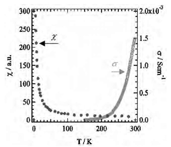
To estimate the electrical conductivity of nanowires, the temperature-dependent electrical conductivity and paramagnetic susceptibility were measured in the form of the LB film. Fig. 14 shows the temperature-dependent electrical conductivity (right scale) and paramagnetic susceptibility (left scale) of LB film of (1)(F4-TCNQ)2. The room-temperature electrical conductivity (sRT) was 1.5 x 10— 3 S cm— 1 with an activation energy of 0.17 eV. The semiconducting temperature dependence was consistent with that of the mixed-stack arrangement of donor and F4-TCNQ dimer. Although the accumulated film should be composed of piles of nanowires and monolayers of (1)(F4-TCNQ)2, each nanowire may have the same order of electrical conductivity.
Fig. 13 Possible molecular arrangements within a nanowire.
The temperature-dependent paramagnetic susceptibility (w) of the LB films of (1)(F4-TCNQ)2 was measured via electron spin resonance (ESR). As shown in Fig. 14, w increased monotonically with decreasing temperatures, which followed the Curie-Weiss law. The line-shape of the ESR signals could be fitted using Lorentzian. Line width around 0.5 mT did not show anomaly within the measured temperature range. Because g-values for BEDT-TTF+ cation and F4-TCNQ— anion radicals have been typically observed at 2.0074 and 2.0025, respective-ly,[11-15] the g-values (~ 2.004) of the LB films for (1)(F4-TCNQ)2 were observed in the intermediate range between BEDT-TTF and F4-TCNQ, which indicated that both the cation and the anion radical species contribute to the paramagnetic susceptibility of the LB films.
Fig. 14 Temperature-dependent electrical conductivity (right scale) and paramagnetic susceptibility (left scale) of the LB film of (1)(F4-TCNQ)2.
CONCLUSION
We constructed oriented molecular-assembly nanowires, which are important parts for the fabrication of nano-scale electronic devices. Molecular-assembly nanowires have a potential to fabricate nanoscale electronics in all self-assembly chemical processes. Amphiphilic bis(TTF) macrocycle derivative is one such example, forming self-assembly nanowires oriented on mica surface. This molecule was designed from the viewpoints of: 1) molecular conductor; 2) Langmuir-Blodgett films; and 3) supramolecular chemistry. Designs from the concepts of molecular conductor and Langmuir-Blodgett film are necessary to construct nanoscale electrical conducting, one-dimensional structure. Furthermore, the design of weak intermolecular interactions (ion recognition) from the supramolecular approach should be a key methodology to construct oriented molecular-assembly nanowires. Control of electronic structures of the nanowires may be achieved through careful design of the charge-transfer interactions (electronic dimensionality, bandwidth, carrier concentration, etc.), while a variety of nanoscale structures such as zero-dimensional nanodots and nano-wires should be obtainable from the designs of supra-molecular chemistry.
