Irradiation Effects Studies
Generally, in situ studies of irradiation effects require somewhat specialized electron microscopes. Because displacement thresholds by electrons, in terms of incident electron energies, vary from 0.1 MeV or less for oxygen in some oxides to more than 1.5 MeV for large atomic number elements, HVEM have routinely been used for such studies since their introduction in the 1960s. For electrons in this range of energies, damage consists largely of single Frenkel pairs (vacancy-interstitial pairs). Since 1961 when the first observations of unintentional in situ ion damage were reported in Au in an 80-kV TEM, due to negative ions desorbed from the microscope’s electron source, in situ TEM studies of ion irradiation effects have become well established for both fundamental and applied irradiation effects research. While the field is often associated with nuclear science and technology, it is relevant to other areas as well such as degradation of microelectronic components in radiation environments, and doping and creation of buried layers by ion implantation in semiconductors. Ion implantation and its associated damage consists of implanted atoms and cascades of point defect clusters which may collapse to form voids or other 3-D defects or partial dislocations which may have profound effects on physical properties. In situ ion beam-related studies require the integration of the microscope and one or more ion sources or ion accelerators, more than a dozen of which have been constructed, mostly in Japan with one in France and two in the United States, involving ion sources ranging from a focused ion beam (FIB) source to a 2-MV tandem accelerator. Two of the Japanese HVEMs employ two ion accelerators each for simultaneous dual ion experiments. In order to do quantitative work in this area, electron and/or ion beam dosimetry, employing miniaturized Faraday cups and effectively performed at or near the specimen position, is a standard requirement.[11,12]
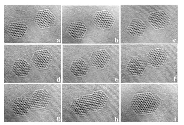
A simple example of a study involving high-energy electrons as the stimulus is shown in Fig. 11. The initial specimen was prepared by implantation of Xe in Al at room temperature. The Xe is very insoluble in the Al matrix and precipitates as nanocrystals, provided they are less than about 10 nm in diameter (at larger sizes the Xe precipitates are fluid). Two such Xe crystals are shown at high resolution in Fig. 11 under 1-MeV electron irradiation in an HVEM, the series of images having been grabbed from videotape. In the sequence, the precipitates experience significant shape changes that lead to their migration. Immediately prior to their coalescence, the precipitates remain with a single plane of Al atoms separating them for several tens of seconds, indicating an absence of elastic interaction of the precipitates. Following coalescence, the resultant precipitate tends to spheroid-ize as one would expect. Such precipitates of gases in metals appear to grow only by migration and coalescence, as opposed to Ostwald ripening characteristic of purely metallic systems, an important fact which was not heretofore factored into simulations of life expectancies of nuclear reactor materials. In related experiments with the Xe-Al system, the absolute values of {100} and {111} Xe/Al interface tensions were determined and ordering at fluid Xe/solid Al interfaces demonstrated.1-13-15-1
Fig. 11 Migration and coalescence of two isolated crystalline Xe precipitates during continuous 1-MeV electron irradiation. Measured from the first image, the elapsed times at which video frames were recorded are (a) 0, (b) 101, (c) 418, (d) 549, (e) 550, (f) 551, (g) 561, (h) 584, and (i) 727 sec.
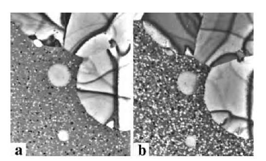
Fig. 12 shows two TEM images from an ion irradiation-induced crystalline study of CoSi2, a material studied extensively as a buried layer in Si. In this study Co and Si were coevaporated onto a thin silicon nitride substrate to produce noncrystalline CoSi2, which was then heated in the TEM to partially crystallize it (the large ”spheres” in Fig. 12). It was then subjected to 1.5-MeV Kr irradiation in situ at room temperature, causing additional fine nucleation and growth of crystals (the tiny spheres) during formation and recovery of the cascades of point defects produced by the ions. Fig. 12 shows the ion-stimulated crystallization process at two stages during continuous irradiation. From such in situ experiments one may determine the ion-induced nucleation and growth rates for the particular irradiation conditions and explore the dependence of these kinetic processes on ion mass and energy which result in different cascade structures.1-16-1
Quantum Dot and Thin Film Growth Studies
The first example is that of growth of quantum dots of Ge on Si. During lattice mismatched epitaxy a range of interesting structures can form spontaneously in order to minimize the total strain and surface energies. In many semiconductor systems having moderate lattice mismatch, greater than about 2%, a common growth mode is the formation of individual, coherently strained 3-D islands. The material at the top of the islands is partially elastically relaxed, reducing the total energy although the surface area of the system increases. For a lattice mismatch of several percent the islands formed have dimensions in the nanoscale regime (up to several tens of nanometers) and this restricted size can lead to interesting optical and electronic properties. This makes such self-assembled islands, or quantum dots, interesting for a range of applications from solid-state lasers to quantum cellular automata.
Fig. 12 Ion-irradiation-assisted crystallization of CoSi2 thin film at 300 K (fine dispersion of crystals), following in situ partial thermal crystallization (massive crystals; the medium-sized sphere near the middle is 500 nm in diameter). Specimen has been irradiated with 1.5 MeV Kr to (a) 3.4 x 10¹⁸ and (b) 8.5 x 10¹⁸ m-2 at 300 K in an HVEM.
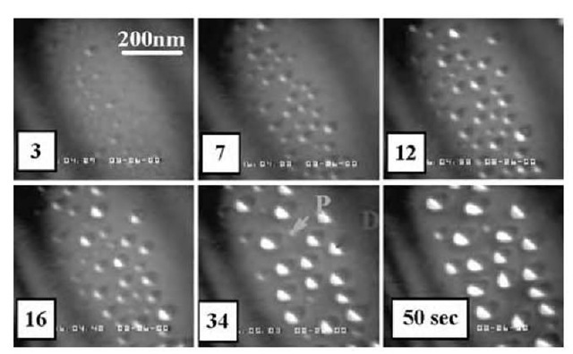
To understand the growth process, island self-assembly in Ge on Si was examined in real time in the TEM. Ge was grown in situ by CVD onto Si (001) at a specimen temperature of 650°C using digermane gas (Ge2H6). A weak beam (dark field) imaging condition was chosen which revealed the strain field around each island. This allowed island positions and sizes to be determined, although the images do not show well the shapes of individual islands. The in situ observations reveal a rich evolutionary process as shown in Fig. 13. After nucle-ation, a bimodal distribution of sizes consisting of domes and pyramids is visible; later the smaller (pyramid) peak almost disappears.
A simple model was developed based on the existence of the two island shapes. During growth, islands can exchange Ge atoms by surface diffusion. If one island, due to its shape or size, has a lower energy per atom than another island, Ge atoms will preferentially detach from higher energy islands and attach to the lower energy island. Islands thus shrink or grow depending on their energy per atom in comparison to other islands in the neighborhood. If all islands were the same shape, larger islands would always have a lower energy per atom than smaller ones by virtue of their lower surface energy/ volume ratio. Larger islands would grow at the expense of smaller ones (Ostwald ripening). However, if two different island shapes are allowed, the process becomes much more complex and interesting. In the model, islands reaching a critical volume make the transition from pyramids to domes and rapidly grow at the expense of smaller pyramids. These real-time TEM observations, therefore, have led to a kinetic model for island growth that predicts how best to control island size and shape given the kinetic nature of the process so that uniformly sized island arrays may be grown. Island positioning now remains the greatest challenge to the use of self-assembled islands in novel devices, and in situ TEM can also be used to investigate the effects on island nucleation of chemical and topographic patterning of the substrate (Frances Ross, private communication, 2003).
Fig. 13 The evolution of Ge islands growing on a thin Si(001) substrate by in situ CVD at 650°C in a TEM. By 3 sec, nucleation of islands is evident, which coarsens with time; after 16 sec a transition occurs in which steep-walled domes form at the expense of shrinking shallow pyramids.
By way of introduction to the second example, the relaxation of strain in semiconductor heterostructures is frequently accomplished by the deposition of misfit dislocation segments at the interface between the hetero-epitaxial layer and the growth substrate when the film is sufficiently highly strained. These dislocations must first nucleate and then propagate to the interface. However, as the dislocations move through the film, they will likely interact with other, preexisting interfacial misfit dislocation segments. If the level of strain in the heterolayer is high, these interactions will not block the motion of the moving ‘threading’ portion of the dislocations. However, when the epitaxial strain is lower, the preexisting inter-facial misfit segments may block the threading dislocations. This limits the ability of the film to relax; these threading segments deleteriously affect the electronic performance of heterostructure devices.
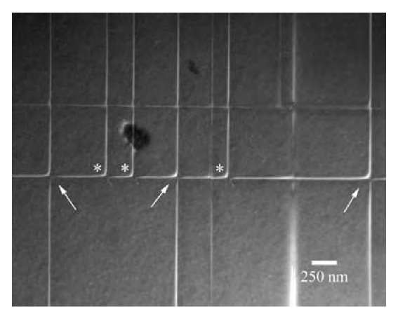
In situ TEM techniques were used to investigate how individual dislocations interact during growth and annealing in strained layer heterostructures. SiGe films of varying composition and thickness were deposited onto clean Si substrates in situ in the modified ultrahigh vacuum TEM of the previous example. This allows the real-time observation of the nucleation, propagation, and interaction of dislocations during strain relaxation, an example of which is shown in Fig. 14. The experimental observations indicated that at very low levels of hetero-epitaxial strain, all dislocations become blocked as a result of interactions, whereas for a regime at higher levels of strain, only dislocations with parallel Burgers vectors may become blocked during interactions, as illustrated in Fig. 14 (at the arrows). Computational simulations indicated that dislocation reactions that occur between dislocations with parallel Burgers vectors result in a stable configuration, and that the stability of this configuration is a function not only of the Burgers vector combination, but also of the direction of approach of the dislocations.[17,18]
Fig. 14 Dark field TEM micrograph from an in situ study of dislocation interactions during recovery in a strained 70-nm-thick Si80Ge20/Si (001) heterostructure. Dislocation pairs of identical Burgers character are indicated by an asterisk if the reaction results in blocking and by an arrow for cases in which interaction does not produce blocking.
A Comment on Specialized Apparatus for In Situ Studies
While the most common in situ studies may involve only heating or cooling of the specimen, several pieces of more specialized apparatus have already been mentioned in conjunction with the specific studies cited above. These include specimen holders which 1) allow application of a magnetic field of known strength and direction, 2) incorporate piezoelectric positioning of some component of an experiment (technology borrowed from scanning probe microscope technology), and 3) incorporate MEMS-type devices for mechanical testing of thin films, nanowires, and the like. At the other extreme of size and investment are microscopes largely dedicated to in situ studies in ultrahigh vacuum or in other environments and to studies involving irradiation effects. The latter may involve connection of an ion accelerator or other radiation source to a microscope with devices for irradiation do-simetry near the position of the specimen.[12] What sets these types of studies apart from their ex situ counterparts is the value-added advantage afforded by the simultaneous availability of a variety of imaging, electron scattering, and chemical and elemental analytical techniques while the specimen is being stimulated in appropriate ways. The possibilities for designing and performing in situ studies are limited largely by the imagination of the investigator.
ANALYTICAL TECHNIQUES SUITABLE FOR IN SITU STUDIES
The extent to which a particular analytical technique or material property measurement method is useful for in situ applications depends largely on the time resolution required per meaningful observation. As a simple example, imagine that one wishes to study Brownian motion of 5-nm Au particles on (0001) graphite in an SEM with field emission gun (FEG). At video scan rates the spatial resolution may be worse than the size of the objects to be observed, and at slow high-resolution rates perhaps the particles move 10 nm on average over the course of a 30-sec exposure scan, for which the effective frame rate is reduced by a factor of nearly 900. Perhaps some intermediate conditions would be suitable, of course. On the other hand, in a conventional TEM it is likely that such observations would be possible at video frame rates at a resolution of 1 nm or better. In TEM the image of the entire area of view is formed at once. Unfortunately, even in this case the recording is not instantaneous though. This example points out the first two factors that are important in conducting in situ studies: the basic instrument in which the experiment is to be conducted and the space/time capabilities of instrumentation for recording the relevant experimental information. The third important factor is the specimen itself. In the case of the SEM experiment the single-crystal graphite substrate could be relatively thick, several micrometers for example, whereas in the TEM experiment the substrate would have to be electron transparent, several tens of nanometers, for example; the thinner the better from a resolution point of view. Finally, in general, if the experimental observations involve imaging, it is important to remember that TEM images are formed in parallel (i.e., all pixels of a given image develop at the same time as mentioned above) whereas in both SEM and STEM, images are formed serially as the area of observation is repetitively scanned. This is not to say that SEM and STEM are categorically inappropriate instruments in which to conduct in situ studies; the choice of instrument largely depends on the nature of the study and the time resolution required in relation to the spatial resolution required.
While it is common and not improper to call SEMs, TEMs, and STEMs microscopies, their several image forming modes of operation are by no means their only modes of operation. For simplicity the other modes may be lumped into two categories, namely, electron scattering and other analytical modes corresponding to various signals from a material specimen resulting from interactions of the incident electron beam with the specimen. These signals may include secondary and Auger electrons, back scattered electrons, visible light and characteristic X-rays as useful signals in the case of SEM, and transmitted electrons, elastically and inelastically scattered electrons, Auger electrons, visible light, and characteristic and diffuse X-rays in the cases of TEM and STEM. A host of specific analytical techniques using these signals have been developed over the past decades as the sophistication of instrumentation has evolved. A number of these are summarized in Table 2, which is not all inclusive. Acronyms for techniques that lend themselves to at least some real-time studies are emphasized in bold. Few of these have been extensively exploited for in situ studies, however.
Table 2 Analytical functions for various operational modes for SEM, TEM, and STEMa
|
Category |
|
Specific operational mode |
|
|
SEM |
TEM |
STEM |
|
|
Imaging |
SEI, BEI, SC, VCI, |
BF, DF, HREM, |
BF, DF, HAADF LSTEM, |
|
VPSEM, LM, OIM , SI, CL |
LM, EFI, |
SI, EFI OIM, SEI, BEI |
|
|
Diffraction |
(BS)ECP |
SAD, CBED, RHEED, |
PRD |
|
EFED |
|||
|
Elemental microanalysis |
(X)EDS, SI, AES, WDS |
(X)EDS, SI, EELS |
(X)EDS, SI, EELS |
|
Chemical analysis (DOS) |
AES |
EELS, AES, ELNES, |
EELS, AES, ELNES |
|
EXELFS |
|||
|
Atom site location |
EXELFS, HREM |
ALCHEMI, EXELFS, |
|
|
HAREXCS, HAADF |
ALCHEMI, atom location by channeling-enhanced microanalysis; BF, bright field imaging; AES, Auger electron spectroscopy; (BS)ECP, (back scattered) electron channeling pattern; BEI, back scattered electron imaging; CBED, convergent beam electron diffraction; CL, cathodoluminescence; DF, dark field imaging; DOS, density of states; (X)EDS, (X-ray) energy dispersive spectroscopy; EELS, electron energy loss spectroscopy; EFED. energy filtered electron diffraction; EFI, energy filtered imaging; ELNES, energy loss near edge fine structure; EXELFS, extended energy loss fine structure; HAADF, high angle annular dark field; HAREXCS, high angular resolution electron channeling X-ray spectroscopy (based on PRD); HREM, high-resolution (transmission) electron microscopy; LM, Lorentz microscopy; LSTEM, Lorentz STEM; OIM, orientation imaging microscopy (based on BSECP); PRD, position-resolved diffraction; RHEED, reflection high energy electron diffraction; SAD, selected area diffraction; SC, specimen current; SEI, secondary electron imaging; SI, spectrum imaging (or elemental mapping); VCI, voltage contrast imaging; VPSEM (or ESEM), variable pressure (or environmental) SEM; WDS, wavelength dispersive (X-ray) spectrometry. aSpecific modes that may be more suitable for in situ studies are shown in bold.
As indicated in Table 2, in TEM and STEM the addition of (electron) energy filtering capability, in column or post column, further enhances the quantitative and aesthetic value for nearly all those analytical techniques involving electrons directly, i.e., bright and dark field imaging, electron scattering, and electron energy loss mapping and spectroscopy.
IMPACT OF ABERRATION CORRECTION OF ELECTRON OPTICS ON IN SITU MICROSCOPIES
With the exception of electron guns and stigmators, which incorporate electrostatic elements, all electron optical lenses in commercial electron microscopes have been electromagnetic (magnetic fields) with cylindrical symmetry (”round lenses”) which unavoidably suffer from positive spherical aberration[19] as well as the other resolution-limiting aberrations familiar in light optics.[20] However, whereas in conventional light optics spatial resolution for imaging (minimum separation of two objects which are distinguishable) is diffraction or wavelength-limited to a few hundred nanometers, in electron optics for which wavelengths are very short (for 100 kV electrons, 3.7 pm) ultimate spatial resolutions are aberration-limited, usually to a few tenths of nanometers for 100 kV, for example.
For some years, several electron optical aberrations— 1) defocus, 2) twofold astigmatism, and 3) axial coma— have been routinely correctable by varying 1) the objective lens current (imaging modes in TEM, STEM, and SEM) or diffraction lens current (diffraction modes in TEM); 2) a biasing field of a weak magnetic octopole within the objective lens (imaging modes in TEM, STEM, and SEM) or diffraction lens (diffraction modes in TEM) which corrects astigmatism introduced by the specimen and objective aperture as well as that of the lens; and 3) accurate correction of beam tilt with respect to the optic axis of the objective lens (especially high-resolution imaging modes in TEM or STEM).
In the past for high-resolution TEM (HREM), the effects of (third-order axial) spherical aberration (described by the coefficient of spherical aberration Cs or C3) have been partially mitigated to achieve improved spatial resolution by choosing defocus of the objective to optimize phase contrast, known as Scherzer defocus,[21] or to minimize the disk of least confusion, known as focus of least confusion.[22] Successful demonstration in the 1990s of hardware correctors for Cs has spurred commercial development of a number of aberration correction systems for electron microscopes based on combinations of electrostatic and magnetostatic hexapole and octupole elements of variable strength. While the concept was introduced 40 years earlier, its realization depended on more recent development of high-speed computer capability and of CCD cameras for execution of the necessary involved, iterative alignment procedures for the corrector elements with respect to one another and with respect to the round lenses of the instrument. The other critical element is the development of current and high-voltage power supplies of significantly improved stability. By 2003, point-to-point resolution for imaging in TEM at Scherzer defocus was improved from 0.24 to ~ 0.13 nm at 200 kV. The correction of Cs in TEM, STEM, and SEM is achieved with assemblies of multipole electrostatic elements, rendering Cs a free parameter of the instrument (like defocus) rather than a fixed property of the objective lens. In addition, for high-resolution imaging in a Cs-corrected TEM, it is possible to partially mitigate the next higher order spherical aberration coefficient for the instrument (C5) by choosing a slightly negative value for Cs for the corrected objective lens.
These continuing developments of aberration correction systems impact ultimate instrumental resolution both for imaging and microanalysis (or more appropriately nanoanalysis) and for in situ applications.1-23-1 In the case of in situ TEM, correction of Cs allows more space around the specimen, into which experimental devices may be incorporated. Previously, increased space was achieved by employing instruments with shorter wavelength electron sources, namely, HVEM, spatial resolution being proportional to Cs14/3. However, in the cases of conventional HVEM and Cs-corrected TEM, spatial resolution remains a sensitive function of the objective lens focal length (gap size in a side-entry objective) due to chromatic aberration associated with high voltage and lens current instabilities (characterized by Cc). For example, in an uncorrected TEM, spatial resolution for imaging of magnetic structures (Lorentz microscopy) is about 2 nm. With both Cs and Cc correction, it should be possible to improve this by an order of magnitude in an experimental space several centimeters in every dimension (Bernd Kabius, private communication, 2003). Furthermore, Cc correction regains some of the advantage of greater penetrating power associated with higher voltage TEM for thicker specimens. Inelastic scattering for thicker specimens diminishes the information limit; this can be compensated by correcting Cc. The development of correction not only for spherical but for chromatic aberration as well should provide, therefore, a strong stimulus for both superb imaging and other analytical functions and for much improved in situ capabilities, in TEM, STEM, and SEM.
CONCLUSION
Over the past several decades, in situ techniques applied to various electron microscopies have contributed extensively to our current understanding of dynamic processes in the areas of materials science and engineering and materials physics. This trend should thrive in the environment of nanoscience and nanotechnology in the future as well, as new and improved instrumentation and experimental techniques, as well as existing analytical techniques which have not been extensively exploited yet, are conceived and brought to bear on the many materials and material systems problems ahead. Performing studies in situ can be a very efficient way to get the job done and, in addition, oftentimes provide an entirely new insight and understanding to physical processes and mechanisms. The possibilities for designing and performing such in situ studies are limited largely by our imaginations.


