INTRODUCTION
The Nobel Prize winning discovery of fullerenes[1] initiated a new era in carbon chemistry. In addition to the two well-known allotropes, graphite and diamond, a large number of carbon structures were synthesized.[2-7] Here we will first discuss the structure of single- and multiwalled nanotubes and the nanotube ”ropes.” The fullerene molecule (primarily the most abundant fullerene, C60), the polymerized, and doped fullerenes will be considered. We will review some of the physical properties, mostly focusing on the electronic structure: electrical conduction, superconductivity, and magnetism.
MOLECULAR STRUCTURE
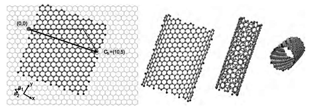
Conceptually, the new structures1-1-7-1 can be derived from graphene, an sp2-bonded honeycomb lattice of carbon atoms, which is the basic element in the structure of graphite.[8] Assume each carbon atom is connected to three neighbors, the bond lengths are fixed to be the same, but the bound angles are a bit variable. If a long strip of graphene is cut out and bent into a cylinder, so that loose carbon bonds match up, we get a nanotube. The matching carbon atoms can be labeled by a chiral vector Ch. This vector is represented by two basic vectors (a1 and a2) and by two integers (n1 and n2); Ch=n1a1 + n2a2 (Fig. 2). Accordingly, the structure of every nanotube is unambiguously characterized by the Ch vector; in a shorthand notation Ch = (n1, n2), so that n1 > n2. Based on the patterns visible on the nanotube they may be called ”zigzag” (for n2=0; Fig. 1), ”armchair” (for n1= n2), or ”chiral” (for any other, see, for example, Fig. 2.). The diameter of the nanotube is given by d = (a/p) [3(n1+n1n2+n2)]1/2, where a=0.144 nm is the carbon-carbon distance. There is no upper limit on the size of the nanotube, although at large diameter the structure becomes very soft [except for multiwalled nanotubes (MWNT), see later]. For small diameter the carbon-carbon bonds are more strained, and the thinnest stable nanotube corresponds to Ch=(5,5) (Fig. 3).
The nanotubes derived from a single graphene strip are called single-walled nanotubes (SWNT).[4,5] If a set of subsequently smaller diameter nanotubes are stacked likeconcentric cylinders, a MWNT is obtained. The distance between the carbon layers in an MWNT is about the same as the distance between the graphene layers in graphite. MWNTs are produced more commonly, and the very first report of nanotubes by Iijima was about MWNTs.[3]
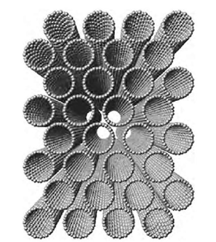
A nanotube rope[10] is a parallel arrangement of SWNTs in a crystalline order, as shown in Fig. 4. The rope is held together by weak van der Waals forces (just like graphite), but it is extremely strong along the long the direction. SWNT strands as long as a few centimeters have been produced.[11]
Fullerenes can be viewed as fully closed graphene sheets. The guiding principle is that each carbon atom is connected to three neighbors, and the bond angles must remain close to 120°. The perfect honeycomb lattice satisfies this requirement, as the building blocks are ideal hexagons. However, in order to get closed surfaces, one has to allow for an occasional pentagon in the structure, just as in the domes designed by the architect Buckminster Fuller (hence are the names of ”fullerene” and ”bucky-ball”). There is a simple geometrical principle, Euler’s theorem, that connects the number of faces (f), vortices (v), and edges (e) of a closed three-dimensional polyhedron, f+ v—e=2. If only hexagons and pentagons are allowed, one can easily prove that the number of pentagons is always 12.
The smallest fullerene, C36, has the shape of a dodecahedron, with exactly 12 pentagons, and no hexagons. However, this molecule is very reactive,[12] as the bond angles are quite stretched. If we look for surfaces where no two pentagons can be nearest neighbor we get the smallest and most abundant stable fullerene, C60 (Fig. 1). In this molecule the carbon nuclei reside on a sphere of about 0.7 nm diameter, with the electronic wavefunctions extending inside and outside by about 0.15 nm. The diameter of the molecule is approximately 1.0 nm, and there is a 0.4-nm-diameter cavity inside. This molecule still has the same symmetry properties as the dodecahedron (described by the icosahedral symmetry group, Ih), and the symmetry is preserved even if not all bond lengths are exactly the same. In fact, in C60 the edges that separate two hexagonal faces are slightly shorter (0.140 nm) than the edges separating a pentagonal and a hexagonal face (0.146 nm). The chemical bond along the shorter edge is sometimes considered double bond,whereas the others are single bonds. Notice, however, the single bond distance in diamond is 0.154 nm (much longer than 0.146 nm), and the typical double bond in molecules is 0.135 nm (much shorter than 0.140 nm). This already indicates that the simple bond picture does not work for C60, and the p electrons are, at least partially, delocalized.
Fig. 1 Four carbon structures, representing diamond, graphite, a typical fullerene (C60), and a typical nanotube (10,0 zigzag, see discussion later).
The most abundant fullerene higher than C60 is C70. Its structure can be constructed by adding a ”belt” of five hexagons in one of the equatorial planes of C60. Other fullerenes, such as C76, C78, C80, and up, have also been prepared and purified. The number of isomers increases rapidly with the increasing fullerene size, representing some difficulty for the determination of their structure (mainly by NMR measurements and theoretical calculations). It is interesting to note that one of the isomers of C80 has the exact shape of an icosahedron (there are also six other isomers with lower symmetry).
Nanotubes with closed ends can be obtained by capping the open ends with a fullerene fragment of appropriate size and shape. For example, the (5,5) nanotube can be capped at the two ends with the two halves of a C60 molecule. Adding more ”belts” of hexagons to C70 yields the same structure. In this sense the distinction between nanotubes and fullerenes is somewhat artificial.
Fig. 3 Scanning tunneling microscope image of a nanotube. The peaks correspond to individual carbon atoms; the chirality of the structure is quite visible.
SYNTHESIS
Once synthesized in the laboratory, fullerenes were also discovered in common sooth and in natural minerals, but it is still more productive to make them in the laboratory. The most common way of preparing fullerenes and nanotubes is the arc discharge method. The typical apparatus[2] consists of a high current source (e.g., and arc welding machine) and a vacuum jar, where a partial pressure (about 100-200 Torr) of He is maintained. Inside the jar two carbon rods are brought into contact to form an arc. A constant distance should be maintained between the rods as the material is gradually converted into carbon sooth. In one version of the apparatus the weight of one of the carbon rods maintains a loose contact between the rods. The sooth is collected from the inside surface of the jar, and from other parts.
Fig. 2 Schematic illustration of deriving a nanotube structure from graphene. The unit vectors and a2, and the chiral vector Ch are indicated in the first panel. Bending the graphene strip results in the nanotube shown in the last panel.
A more precisely controlled preparation method involves laser ablation of carbon.[1'10] The graphite target is kept at high temperature (1200°C) in a furnace. A high power laser (typically a Nd:YAG laser operating at several hundred millijoules of power) is aimed at the target and produces a carbon plasma. A flow of inert gas carries the end products and deposits them in a colder part of the apparatus.
In both cases the reaction products are mixtures of various fullerenes, nanotubes, and amorphous carbon, although by properly setting and controlling the preparation conditions the relative quantity of the end products can be influenced greatly. Nevertheless, the separation and purification of the components is a critical part of the process. Various organic solvents (such as toluene or tetrahydrofurane) can be used to dissolve fullerenes or disperse the nanotubes. High-performance liquid chroma-tography (HPLC) is used to separate the different fractions. Once a solid phase is obtained fullerenes can be further purified by sublimation (e.g., C60 sublimes at 430°C). Smaller quantities of higher fullerenes can also be purified by gas-phase separation methods.
Fig. 4 Cross-sectional view of a nanotube rope.
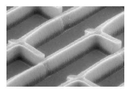
Fig. 5 Nanotubes grown by chemical vapor deposition on a pattern of catalyst deposited on a substrate.
A third approach, primarily used in the production of SWNTs, is based on chemical vapor deposition (CVD). This method involves a carefully prepared catalyst, and it can be used to grow large quantities of ordered nano-tubes.[13] It is generally believed that SWNTs are more readily obtained if the reaction temperature is not too high. Note that in the arc discharge method the reaction happens at temperatures larger than 3000°C, whereas in CVD the temperature of the reaction can be kept below 1000°C. Fig. 5 shows a pattern of ”nanotube forest” synthesized by CVD.
MOLECULAR PROPERTIES
The unsaturated nature of the sp2 bonds is responsible for several interesting properties of fullerenes and nanotubes. Functionalization (attaching other molecules with desirable properties) can be carried out easily. A pretty good description of the electronic properties can be obtained by assuming that three of the four valence electrons of each carbon are tied up in the three a bonds, and by considering the behavior of the remaining one electron. There is a large body of literature dealing with these issues (see, for example, Refs. [6] and [7]); we will focus on one of the fullerenes, C60. We will also discuss the electronic states in a single SWNT.
Electronic States in C6o
C60 has 240 valence electrons, but each carbon atom has three sigma bonds to its neighbors, using up a total of 180 electrons for this purpose. The energy of these electrons is well below the Fermi surface. They stabilize the structure, but they will not contribute to the conduction. The remaining 60 electrons are distributed around the molecule on orbitals that originate from the (much less tight) carbon-carbon p orbitals. There are two important differences between these orbitals and the p electrons of a graphene plane. First, the three bonds around a carbon atom in C60 (or in any other fullerene) do not make a plane. Whereas in graphene the electrons had equal probability of being ”below” and ”above” the plane, in fullerenes the p electrons tend to spend more time outside of the ball than inside. Second, in C60 the C-C bond lengths are not uniform, the p electrons are not truly delocalized around the six-member carbon rings (like in benzene or graphene), but they are distributed over 30 ”bulges” of electronic orbits that stick out of the C60 molecule. A somewhat lower electron density belongs to the other 60 orbits connecting the carbon pairs with longer bond lengths.
The first insight to the nature of the molecular orbitals can be obtained by borrowing ideas from the early days of nuclear physics, when the quantum mechanics of particles confined into a spherical potential well was first considered. In this case the states are still labeled by quantum numbers n, l, and m, just like in the hydrogen atom, but the peculiar degeneracy of the different angular momentum states, which characterizes the textbook treatment of the hydrogen atom, does not apply. In steep-walled potential well (like in a nucleus or in a C60 molecule) the lower l states will have lower energy.
Let us consider 60, noninteracting electrons, confined to a sphere on a high n orbit with various l’s. The first two electrons will fill up l =0 state. Proceeding to higher l, one has to count the number of available states, N =2(2l+l) (where the first factor of 2 stands for spin). It is easy to see that by reaching l=4 altogether 50 electrons are consumed. The remaining l0 electrons will all go to the l=5 state.
In reality the situation is much more complex. The potential does not have the spherical symmetry; each carbon atom creates its own potential well for the electrons. Nevertheless, a more exact treatment of the electrons (e.g., a Hiickel molecular orbital calculation) shows that the above arguments work well for l=0,1,2,3,4. For higher energies the ”spherical potential” approximation does not work anymore. In order to go any further we need to look at the energy splitting due to the true atomic potentials. In the real C60 l is not a good quantum number, and the electronic orbitals should be labeled according to the irreducible representations of the icosahedral symmetry group. The orbitals available for the remaining l0 electrons are, in the order of increasing energy, the hu, the f1u, and the f1g levels. The degeneracy of these levels (including spin) is 10, 6, and 6, respectively. The hu level is completely filled by the 10 remaining electrons, becoming the highest occupied molecular orbit (HOMO), and the f1u level becomes the lowest unoccupied molecular orbit (LUMO). The HOMO-LUMO gap is about 2 eV.
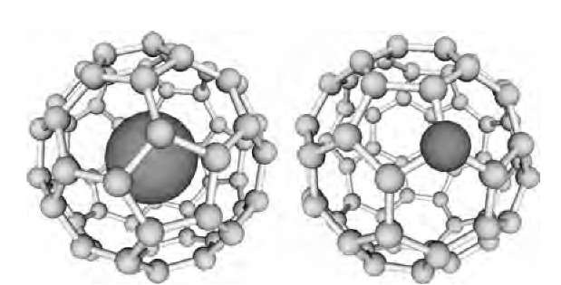
The energy gap between the filled and empty electronic states causes the molecule to be nonreactive, and it accounts for the insulating nature of the C60 solid. The empty f1u level can hold six electrons, and a proper addition of electrons to the molecule (sometimes called ”doping”, in analogy to adding electrons to a pure superconductor) should result in dramatic changes in the properties, including higher reactivity and metallic character. Two possible ways will be discussed here shortly: adding an atom inside the C60 cage (endohedral doping) and exchanging a carbon atom to another one (on-site doping; Fig. 6). The third (and most fruitful) method, exohedral doping, when the donor atom is placed in-between the C60 molecules, will be considered later.
Fig. 6 Endohedral and on-site doping of a C60 molecule.
Endohedral C60 molecules can be prepared by a ”brute-force” method, where ions of atoms are accelerated and implanted to the C60 cage.[14] The ions should have just enough energy to open up the cage and enter. The first collision should absorb and redistribute a good part of the initial kinetic energy so that the atom does not escape the cage. Endohedral molecules of M-C60 with M=N, P, Li, Ca, Na, K, Rb were produced this way in small quantities. A larger yield can be achieved by coevaporation[15] of the carbon and the metal is an arc-discharge chamber (typical for fullerene production). In this process mostly higher endohedral fullerenes, such as M-C82 (where M is a metal atom), can be extracted from the soot on a chromatographic column.
Electron spin resonance spectroscopy (ESR) studies and detailed quantum chemical calculations show that the endohedral dopant atom does not always transfer its charge to the cage. If the dopant remains neutral, it stays in the center of the cage, like in N-C60.[16] Compounds such as La-C60 are very interesting, as complete charge transfer from La to the C60 cage results in a triply charged molecule.
On-ball doping has been achieved by replacing one carbon atom with a nitrogen atom obtaining C59N (azafullerenes).[17] The replacement of N for C adds one extra electron to the cage, changes the structure locally, lowers the symmetry of the molecule, and splits the degeneracy of the electronic orbitals. Furthermore, this chemical substitution renders the molecule very reactive with a high electron affinity. At ambient temperature the C59N exists only in a dimerized phase.
Electrical Conduction in Nanotubes
In order to understand the electrical properties of a nanotube, we first have to look at a single graphene sheet.
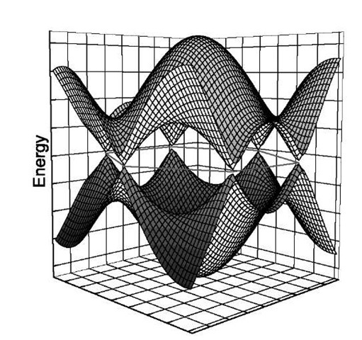
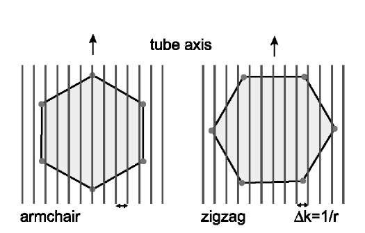
Graphene is on the borderline of being metallic: the band structure calculation results in a ”zero-gap semiconductor” behavior.[18] Fig. 7 shows an illustration of the electron energy as a function of the two-dimensional wave vector. The Brillouin zone of graphene is a hexagon, and the allowed electronic states (wave vectors) correspond to the points inside the hexagon; the electronic bands reach the Fermi level at the six corners of the hexagon. Therefore the Fermi ”surface” consists of six points, as indicated in the two panels in Fig. 8. (In graphite the influence of the neighboring layers causes the bands to cross the Fermi level, and there will be finite Fermi surface, yielding a semimetallic behavior.)
By bending the graphene sheet into a nanotube the most drastic change will be the constraint introduced due to the periodic boundary condition along the circumference of the cylinder. Accordingly, in the direction perpendicular to the tube axis the allowed wave vectors will be constrained to lines. The larger the diameter of the nanotube the more dense are the lines. Naturally, for a very large diameter nanotube the allowed wave vectors are just about the same as for the graphite, and the properties are also similar. However, for smaller diameters the constraint is really important. As shown in the two panels of Fig. 8, the relative orientation of the lines corresponding to the allowed states is sensitive to the actual structure of the nanotube.[8,19] For armchair nano-tubes one of the lines always intersects the corner of the hexagon, therefore these nanotubes are metallic; for the zigzag structure it is possible that the lines miss the corners, and in those cases the nanotube is semiconducting. By carrying out this analysis in more detail, we obtain that a nanotube is metallic if the integers in the chiral vector describing the structure Ch =(n1,n2) satisfy n1 — n2=3j, where j is an arbitrary integer. More detailed calculations, taking into account the curvature of the graphene sheet, lead to the conclusion that for n1 =n2 (armchair) the nanotubes are metallic, for n1 — n2=3j there is a tiny gap at the Fermi surface, and for all other cases the gap is large.
Fig. 7 Schematic representation of the energy bands in graphene. The possible electron states are constrained in a hexagon in the base plane. The lower band is full, the upper band is empty. The energy of the electrons is zero (equal to the Fermi energy) at the six corners of the hexagon.
Fig. 8 The six corners of the hexagon correspond to electronic states available for conduction. The lines represent the allowed electronic states in a zigzag and an armchair nanotube.
Much progress has been made in the experimental test of these predictions.[21] One prefers to work with a SWNT, because for a MWNT it is unlikely that all of the component nanotubes are of the same type (metal or semiconductor). The first conductance measurements were done on a nanotube rope, a collection of similar SWNTs. Several single SWNTs of various chirality have been tested later. The measurements largely support the conclusions drawn above. For the complete interpretation of the experimental results one needs to step beyond the simple theory of bulk metals: the electrical leads to the nanotube must be treated as tunneling contacts. The resonance between higher quantum levels and the Coulomb repulsion of electrons on the nanotube play important roles.[22,23]
FULLERENE SOLID
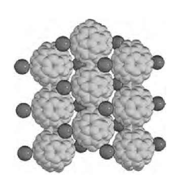
The vast majority of research on the fullerene-based solids was done on C60. The molecule dissolves in various solvents. Crystallization from solution usually yields a structure that includes the solvent molecules.[24] However, sublimation in vacuum or inert gas atmosphere may yield pure C60 crystals of several millimeters or even centimeter size. In the solid form the centers of the fullerene molecules are ordered in a face-centered cubic (fcc) crystal lattice (Fig. 9).
Fig. 9 A pure fullerene crystal, and the illustration of the structure of the fullerene solid.
At room temperature the fullerene molecules rapidly and randomly rotate between various orientations.[25] In time average the molecules look like spheres and all of the molecular sites are equivalent. (The well-definec molecular center and a nearly free molecular rotation are not a unique property of the fullerene molecule. It is characteristic to many organic solids, where the binding is due to van der Waals forces, and the molecule has ”rounded” symmetric shape, like solid CH4 and CCl4.)
The nearest neighbor C60-C60 distance corresponds to the diameter of the molecule. At room temperature the size of the cubic unit cell is 1.417 nm, and the nearest neighbor distance is 1.002 nm. As the temperature is lowered, the rotation of the molecules stops. The center of the molecules remains in about the same place, but the incompatibility of the icosahedral molecular symmetry and the cubic lattice symmetry makes it impossible to describe the structure in terms of the simple fcc lattice, with one C60 molecule of fixed orientation each unit cell. The freezing of the rotational motion actually happens in two stages. First, at 261 K the rotational axis of each molecule becomes constrained. The building block of the new structure consists of four C60 molecules arranged at the vertices of a tetrahedron, with each one of them spinning around a different, but well-defined axis.[26-29] Then, at lower temperatures, the rotation around these axes slows down and stops gradually. Below about 90 K the molecules are entirely frozen, but they never order perfectly.
Doped Fullerenes
The linear size of a fullerene molecule is 10 times larger than a typical atom. Even in a close-packed fcc structure, large empty spaces between the molecules are freely available for smaller atoms, ions, or molecules. Because of the unsaturated character of the C-C bonds on the fullerene, there are plenty of electronic states to accept electrons from appropriate donors. The combination of alkali and alkaline earth elements with fullerenes results in an unusual variety of AnC60 materials that are mostly near-stoichiometric (A can stand for Na, K, Rb, Cs Ca, Sr, and Ba). Organic and inorganic molecules were also used to produce charge transfer salts with fullerenes. The term ”doped fullerene” is often used to describe the product (although in its original sense, ”doping” means a small, nonstoichiometric amount of charge transfer, typically in a semiconductor).
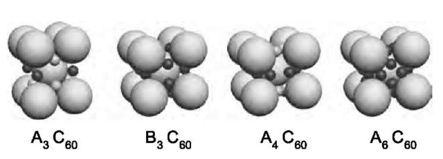
In the fcc structure the interstitial sites have either octahedral or tetrahedral symmetry. The tetrahedral sites are smaller, and there are twice as many of them as octahedral sites. A series of AnC60 (with n=0,1,2,3,4,6,10) materials are based on the original fcc structure of pure C60. Several other compounds are known where the C60 abandons the close-packed structure.[30-35] Two of these, the body-centered tetragonal A4C60 and the body-centered cubic A6C60, are illustrated in Fig. 10. There is also a series of compounds with alkaline earth metals. Based on the simple electron band arguments, the HOMO level of the C60 can accept a total of six electrons. Anything less than that should result in a partially occupied electron band and lead to a metallic behavior in the solid state. Surprisingly, at room temperature and ambient pressure, only AC60, and A3C60 are metals (for a review, see Ref. [34]).
Superconductivity and Magnetism in Fullerenes
A class of alkali-metal-doped fullerenes, with chemical composition A3C60, is metallic at room temperature[36] and turns into superconductor at low temperature.[37] The transition temperature is unusually large; for example, in Rb3C60 it is 32 K.[38] In contrast to other exotic superconductors (such as the copper-oxide-based high-temperature superconductors) the superconductivity in fullerides is well understood in terms of the theory developed in the 1960s by Bardeen, Cooper, and Schrieffer (BCS). The formation of Cooper pairs (two electrons that are held together by some attractive force) is the key element of the BCS theory. In the A3C60 fullerides the conduction electrons are donated by the alkali metal atoms to the C60 molecules, the electrons easily hop between the molecules (because of the overlap of the molecular orbits), and the attractive interaction is mediated by the deformation of the molecule induced by the presence of the electron.
Fig. 10 The leftmost structure corresponds to A3C60, with A = K, Rb, Cs, (or a mixture of these). If the dopant is an alkaline-earth metal (denoted by B), the structure is B3C60. The A4C60 and A6C60 structures shown here are known to exist with A = K, Rb, and Cs.
When C60 is combined with the strong electron acceptor tetrakis(diethylamino)ethylene (TDAE) each fullerene molecule loses an electron. It was expected that this material will also be a metal, and perhaps a superconductor, too. Instead, it turned out to be an insulator, but when it was cooled to low temperature a strong magnetism was detected. (TDAE)C60 is a ferromagnetic compound with a Curie temperature of 16 K.[39,40] It is very rare to find ferromagnetic behavior with no transition metal (such as iron or nickel) in the chemical formula. (TDAE)C60 held the record of being the highest temperature truly organic ferromagnet.
Polymerization of Fullerenes
The ability of the C60 molecule to form covalently bonded polymers was first noticed in laser-irradiated thin films of C60.[41] The polymerization happens in a Diels-Alder-type (2+2) cycloaddition reaction when the double bonds on two fullerenes are broken up and cross links are formed. This reaction has a large activation energy, and at room temperature it is extremely slow. It is believed that (2+2) cycloaddition also occurs in high-pressure/high-temperature polymerization of fullerenes.[42] Some of these high-pressure synthesized disordered polymers are very attractive for applications, as they can exhibit mechanical properties stronger than diamond.
In doped fullerenes polymerization can happen without exposing the material to light, high temperature, or pressure. The best known examples are KC60 and RbC60, where the fullerene molecules form linear chain structures (Fig. 11). The formation of these chains happens spontaneously as the material is cooled slightly below room temperature.[43] There are dramatic changes in the electrical conductivity and in the other properties; most notably the material becomes stable in air (otherwise all alkali-doped fullerene compounds decompose rapidly in air). This is a reversible transition, and the material turns back to the monomeric form if the temperature is raised. A slightly different polymer is formed in Na4C60. In this compound, sheets of C60 molecules are formed so that there is a single bond between the nearest neighbors.
Fig. 11 The low-temperature structure of RbC60. The polymerized C60 chains are quite visible.
CONCLUSION
Inorganic fullerenes and nanotubes have been prepared in binary composition; for example, the graphite-like solid lubricant MoS2 served as the basis for a series of compounds.[44] However, only carbon has the extraordinary chemical flexibility to serve as the sole basic unit of such a variety of compounds. The materials discussed here are testing grounds for important concepts in condensed matter theory; at the same time there is a constant effort to find potentially useful applications. Fullerene-like structures are known in more complex materials, including biologically important molecules, including the HIV virus. C60 was investigated as a potential drug delivery agent, it may have antiviral activity,[45] and endohedral C60 compounds can be possibly used as a spin label (or relaxation agent) in magnetic resonance spectroscopy.[46] Bulk quantities of nanotubes are considered for reinforcement additives in metals and for storage of hydrogen gas.[47] In scanning tunneling and force microscopy the nanotubes may serve as the sharpest possible microscope tip. Single nanotubes were shown to work as single-electron transistors, reaching the ultimate limit of nano-scale electronics.[48,49] Electron emission and light emission from the tips of the nanotubes have been seen at relatively low applied voltages, and according to a recent press release from Motorola, the nanotube-based ”nanoemissive display (NED) technology enables manufacturers to design large flat panel displays that exceed the image quality characteristics of plasma and LCD screens.” The strange structures, discovered during the search for new molecules in the interstellar medium,[1] may have a real impact on our everyday life in the not-too-distant future.


