INTRODUCTION
Nanotechnology[1-5] continues to be a rapidly emerging field in which new ideas are being born and discoveries are being made at a breathtaking pace. New materials systems with novel properties are being designed or invented at an incredible rate in laboratories throughout the world. Of nanosystems, two of the most intensely studied are carbon nanotubes (CNTs)[6'7] and metal-oxide nanoribbons.[8] CNTs have been a popular area of research for more than a decade because of the promise of a host of commercial applications, while metal-oxide nanoribbons, particularly those synthesized from inexpensive SnO2 and ZnO, have been a materials system of great current interest because of their potential applications as chemical sensors for pollutant gas species and biomolecules. The well-characterized atomic structures of both these systems, as well as their high degree of structural purity, allow accurate computer modeling and in silico property prediction. In the following, we illustrate some of the modern techniques of molecular modeling to study technologically important applications such as displays, electromechanical sensing, and chemical sensing.
ROLE OF MOLECULAR MODELING
As with any new technology, Nanotechnology has many challenges to overcome, typically associated with our control and precision at the nanoscale. Some of the challenges include: device integration (interconnect failure, addressability issues), growth and synthesis (difficulty in size-dispersion control, requirement of novel assembly techniques, presence of structural defects), contact resistance (necessity of atomic-level structural precision at junctions), functionalization (challenges with chemical inertness), and doping (nonuniformity of dopant levels). Molecular modeling is a great approach in surmounting some of the above obstacles because it often provides deeper insight into the system properties as a function of size/shape, structural defects, added functional groups, and system surroundings. Often, the whole nanosystem/device can be modeled in full atomistic detail on the computer, and its properties studied with a level of precision not possible experimentally. The growing success of density functional theory (DFT),[9] availability of accurate interatomic potentials (force fields),[10] development of Green’s function-based electronic transport codes,[11] and deployment of sophisticated graphics user interface (GUI) have all led to the emergence of molecular modeling as a powerful tool in Nanotechnology research. Molecular modeling applications to nanomaterials are too numerous to mention here, and we can only point to the literature for further reference.[12-17]
CARBON NANOTUBES (CNTs)
Atomic and Electronic Structure
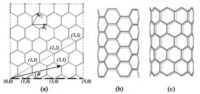
A CNT can be geometrically thought of as a graphite sheet rolled into a seamless cylinder. A necessary condition for the cylinder to be seamless is that, upon rolling, a graphite lattice point (n1,n2) coincides with the origin (0,0). Thus if a1 and a2 are the two lattice vectors of graphite, the CNT circumference is equal to the length of the vector (n1a1 + n2a2), while the CNT chiral angle 0 is defined as the angle between vectors (n1a1 + n2a2) and a1. With the choice of lattice vectors as in Fig. 1a, the chiral angle and diameter of a CNT are given respectively by the formulas:
where a =la1l = la2l ~ 2.45 A is the lattice constant of graphite. The CNT diameter and chirality, and therefore its atomic geometry, are completely specified by the two integers (n1,n2), which are referred to as the chiral indices of the CNT. Because of the symmetry of the graphite lattice, a nanotube of any arbitrary chirality can be defined in the range n1 > n2 > 0 and n1>0, which implies that the chiral angle 0 for all CNTs lies between 0° and 30°. CNTs with the extreme chiral angles of 0° and 30° have special names: a CNT with 0=0 (i.e., n2=0) is called zigzag, while a CNT with 0=30° (n1 = n2) is called armchair. The names armchair and zigzag simply reflect the shape of the open edges of these CNTs (Fig. 1b,c). CNTs with any other chiral angles (i.e., 0 < 8 < 30°) are called chiral.
Fig. 1 Carbon nanotube (CNT) basics. (a) A graphite sheet with lattice vectors a1; a2. A few lattice points are indicated, as is the chiral angle 8 for a (3,1) CNT. Dotted and dashed lines are drawn along circumferences of armchair and zigzag tubes, respectively; (b) a (5,5) armchair tube; (c) a (9,0) zigzag tube.
Armchair and zigzag CNTs possess short periodic repeat lengths along the nanotube axis, the repeat length being only a 2.45 A) for armchair tubes and y/3 a 4.24 A) for zigzag tubes. On the other hand, chiral CNTs can possess very long periodic repeat lengths depending on the ratio of its chiral indices. Thus electronic structure calculations, especially those employing first-principles Quantum Mechanics (QM) with periodic boundary conditions, are rarely performed on chiral tubes. However, this does not turn out to be a serious limitation. Because a CNT is just a rolled-up graphite sheet, one can obtain a good approximation to the CNT electronic structure simply by applying an appropriate boundary condition to the electronic structure of a graphite sheet, with a small perturbation resulting from the finite cylindrical curvature of the CNT surface. The boundary condition for a CNT with chiral indices (n1,n2) corresponds to the coincidence of the (n1,n2) lattice point of graphite with the origin (0,0). It has been known for some time that a single sheet of graphite (also known as graphene) is neither a semiconductor nor a metal, but a semimetal[18] (i.e., a zero-bandgap semiconductor). This peculiarity implies that the electronic states of graphene are very sensitive to additional boundary conditions that a CNT mandates. Taking into account small effects due to curvature, such boundary conditions lead to the important result[19-24] that: all armchair tubes are metallic; CNTs with n1 -n2=3n (n=any positive integer), which includes the (3n,0) zigzag tubes as a special class, are quasimetallic (small bandgap ~ 10 meV or less, arising from curvature effects); and CNTs with n1 -n2^ 3n are semiconducting, with a bandgap decreasing as 1/d as a function of tube diameter d (thereby converging to the zero bandgap of graphite in the limit d!i). Experimental measurements are often unable make the distinction between metallic and quasimetallic tubes because of the presence of contact resistance and thermal effects. Thus, for simplicity, experimentalists often classify CNTs as either metallic or semiconducting, and we follow the same convention in the discussion below.
Synthesis Methods, Properties, Potential Applications
CNTs were originally discovered by Sumio Iijima in 1991[25] in the soot produced by an arc discharge between graphite electrodes in a helium atmosphere. The original tubes[25-27] were multiwalled, i.e., they consisted of several concentric cylinders with successive layers separated by a distance approximately equal to the interlayer spacing of graphite. Subsequently, single-walled CNTs were synthesized in the same arc-discharge apparatus with the addition of transition-metal catalysts.[28,29] Presently, high-quality multiwalled and single-walled CNTs can be grown in well-defined directions via chemical vapor deposition (CVD),[30] while high-yield of single-walled CNTs can be obtained by several techniques, including: arc discharge of Ni-Y catalyzed graphite electrodes,[31] laser ablation of Ni-Co catalyzed graphite targets,[32] and vapor-phase pyrolysis of CO and Fe(CO)5[33] (the so-called HiPCO process).
Over the last decade, CNTs have become one of the hottest research areas in all of science and engineering because of a number of fascinating properties:
Depending on their chiral indices, they can behave like metals or semiconductors, as discussed in the section ”Atomic and Eectronic Structure.”
Single- or multiwalled CNTs are exceptionally strong, could possess a Young’s modulus as high as 1.2 TPa, six times the modulus of steel. CNTs are elastic to the highest degree, and do not display plasticity behavior even under large deformation including stretching, bending, or twisting. Metallic CNT are one-dimensional quantum conductors where electrons travel ballistically: there is no heat dissipation along the length of the CNT. All dissipation occurs at the contacts. CNTs can have huge aspect ratio (i.e., length-to-diameter ratio), as large as 105. Therefore, field emission of electrons can be induced from the tip of long metallic CNTs in the presence of moderate electric fields. Depending on its chiral indices, metallic CNTs can undergo metal-to-semiconductor transition under small tensile or torsional strain. This effect is discussed in more detail in this section. With a magnetic field parallel to its axis, a CNT can exhibit the Aharonov-Bohm effect. Atoms/molecules can be enclosed inside a CNT. A CNT can be doped both p-type and (to a lesser degree) n-type.
All of the above properties come with the promise of a host of commercial applications,[34,35] including: field emission-based flat panel displays,[36-42] novel semiconducting devices and robust metallic interconnects in mi-croelectronics,[43,44] hydrogen storage devices,[45] structural reinforcement agents,[46] chemical sensors,[47-49] electromechanical sensors,[47,50] nanoprobes,[51] and [52] nanotweezers.[52]
Molecular Modeling of CNTs
Ever since they were discovered, CNTs have provided a fertile ground for theoretical simulations and analysis. In fact, the prediction of the dependence of CNT’s electronic structure on its chirality[19-21] came within just a few months of the experimental discovery.[25] Since then, there have been a huge number of theoretical investiga-tions[14-16,53-55] of growth mechanisms, structure and energetics of topological defects, mechanical and electrical response to various kinds physical perturbation, field emission from tips of metallic CNTs, electronic effects of doping and gas adsorption, chemical reactivity, interaction with polymers, capillary effects, CNT-metal contacts, H and Li storage, thermal conductivity, and encapsulation of organic as well as inorganic material. Computational approaches used in the above work include solving diffusion equations, QM simulations (DFT, tight binding, and semiempirical methods), classical molecular dynamics, kinetic Monte Carlo, genetic algorithms, and Green’s function-based electronic transport theory. The following two sections illustrate the use of some of the above techniques to explore two application areas of CNTs: 1) field-emission displays; and 2) nano-electro-mechanical sensors.
CNT-based displays: effect of adsorbates
Synthesis of CNTs with length-to-width ratio as large as 105, as well as advanced fabrication methods for generating self-aligned or patterned nanotube films on glass[56] or silicon[40] substrates have pushed CNT-based flat-panel displays to the brink of commercial reality.[57-59] One major challenge to overcome is to reduce the threshold field, defined as the electric field necessary to induce a current of 1 mA/cm2. One way to achieve this is to introduce adsorbates that might effectively lower the ion-ization potential (IP) and facilitate the extraction of electrons. An important experimental work in this regard was performed at Motorola,[60] which studied changes in field emission behavior in the presence of various gases, i.e., CO, CO2, H2, and water vapor. Adsorbed water was found to significantly enhance the emission current, while the other residual gases did not have any noticeable impact. Water also appeared to be present at the CNT tip up to very high temperatures 900 K), and field-emission current was more enhanced at higher partial pressures of water.
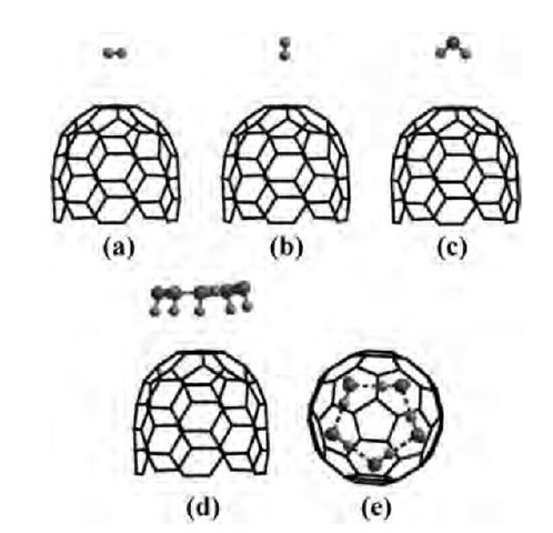
To understand the difference between H2 and water on the field-emission properties of CNTs, first-principles electronic structure calculations were carried out on a (5,5) armchair tube, with a hemispherical tip represented by the half of a C60 molecule. A uniform external field Efe, directed toward the tube from above, was chosen to represent the electric field close to the tube tip under field emission conditions. Because the actual field close to the tip is radial rather than uniform,[61] the uniform field representation is appropriate only if the tube stem in the simulation is confined to the same size as the tube diameter. For this reason, a short stem of three atomic layers (30 atoms) was used. A more realistic field around the tip could perhaps be simulated via a large number of point charges situated at some distance from the tip. Such an effort was not undertaken for two reasons: 1) in all flat panel display designs, the field emission occurs not from isolated tubes, but from a film of closely spaced nearly aligned tubes, with the resulting E-field more closely resembling a uniform field above the tip assembly; 2) the essential chemistry that drives the effect of adsorbates on field emission behavior can be extracted from calculations by using a uniform field, as illustrated below. For all calculations, a magnitude of Efe= 1 V/A was used as a ballpark figure, around which field emission is known to occur for these systems. Difference in electronegativities between H and C introduces an artificial dipole moment in the CNT if the dangling C atoms at the stem end are H-saturated. The C atoms at the stem end were therefore left unsaturated. In addition, these C atoms were fixed during the simulation to mimic the presence of a long stem in actual experiments. Structures of the CNT with or without adsorbates were optimized by using the DFT code DMol3,[62] in which the electronic wave functions are expanded as a linear combination of atom-centered basis functions defined on a numerical grid. The present calculations explicitly considered all electrons in the system (i.e., core electrons were included), with wave functions expanded in the double numeric polarized (DNP) basis set,[63] and the exchange-correlation part of the electron-electron interactions represented by the gradient-corrected Perdew-Burke-Ernzerhof (PBE) functional.[64] The main results from this study[65] can be summarized as follows:
Fig. 2 Optimized structures for adsorbates on a CNT tip in zero electric field: (a) H2 (flat); (b) H2 upright; (c) a single ”down” water; (d) a cluster of five water molecules; (e) view of (d) from top.
1. A single H2 molecule can either lie ”flat” or ”upright” on the CNT (Fig. 2a,b). A single water molecule adsorbs in such a way that its plane symmetrically cuts the CNT into two equal halves. The two H atoms are symmetrically equidistant from the tip, and could be either closer or further from the surface as compared to the O atom. We call these configurations ”down” (Fig. 2c) and ”up” water, respectively.
2. In zero electric field, none of the adsorbates show any significant binding to the CNT tip. The H2 has less than 0.1 kcal/mol binding in either configuration, while a single water has ~ 0.7 kcal/mol binding.
3. At a tip field of 1 V/A, the binding energies change significantly. Thus H2 has a binding energy of 1.1 and 3.5 eV, in the flat and the upright configurations, respectively, while the ”down” water has a binding energy of ~ 20 kcal/mol, which is of the order of a chemical bond. The ”up” water becomes unstable in the presence of a finite electric field at the CNT and spontaneously flips into a ”down” water. Therefore ”up” water is not considered further in the discussion below.
4. Because water molecules can form clusters through H bonding, it was also important to consider the structure and adsorption energy of a cluster of water molecules on the CNT tip. Because of the fivefold symmetry of the (5,5) CNT (with a C60 half cap) about its axis, it was easy to determine the global minimum for a cluster of five water molecules. In the minimum energy structure, the five water molecules form a ”crown” on the top of the CNT (Fig. 2d,e). Each water molecule in this crown is tilted with respect to the ideal ”down” water configuration for a single water molecule. However, the resulting loss in interaction energy with the CNT tip is almost exactly recovered from the gain in H bonding to the nearest neighbor waters.
5. The adsorbate atoms in all cases are at a distance of 3 A or more from the CNT surface. This strongly suggests that they are being physisorbed. This is supported by an analysis of charge density in the region between the adsorbate and the CNT tip, which is less than 0.004 el/A3. Even at a field as large 1 V/A, the changes to the adsorbate and CNT structures are small. In particular, the distance between the adsorbate and the CNT changes by less than 0.07 A, and the bond lengths change by less than 0.01 A. The most significant geometrical change is in the H-O-H angle in water, which decreases from 103.7° in zero field to 98° on the tube tip at Efe= 1 V/A. Such a change in angle leads to only a 0.02 a.u. increase in the dipole moment of water.
6. An analysis of the various interaction energies and the dipole moments of the CNT as well as the adsorbates yield the following picture: in the absence of an electric field, the CNT has a very small dipole moment. This small dipole has only negligible interaction with any of the adsorbates. However, under field-emission conditions, large E-field at the CNT tip induces a significant dipole moment. This dipole interacts with the dipole of the adsorbates. Water molecules having a large intrinsic dipole moment interacts strongly, while H2 molecules have only a small field-induced dipole, and therefore a much weaker interaction.
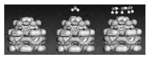
7. Finally, the highest occupied molecular orbital (HOMO) for the isolated CNT, one water molecule on CNT, and five water molecules on the CNT were analyzed (Fig. 3). The HOMO essentially remains confined to the CNT tip, and its shape does not significantly change because of the presence of the adsorbates. However, when the ionization potential (IP) is computed, it is found to be 0.1 and 0.6 eV lower for the one water and five water cases, respectively, compared to the adsorbate-free CNT. This also perfectly correlates to the instability of the HOMO orbital. Thus electrostatic interactions from the adsorbates make the HOMO level in the CNT more unstable, with a corresponding decrease in the IP, thereby lowering the operating voltage for field emission.
Fig. 3 Highest occupied molecular orbital (HOMO) for: isolated CNT; CNT+1 adsorbed water; and CNT+ 5 adsorbed water. Although the position and shape of the HOMO is not significantly affected by the adsorbates, the energy level and ionization potential change markedly.
Table 1 displays computed IP of a (5,5) CNT tip (same as in Fig. 2) for a number of potential adsorbates,[66] including water. It is clear that as the lowering of IP becomes more pronounced, the larger the dipole moment of the adsorbate becomes. This work calls for further experiments on polar adsorbates to optimize the performance of CNT-based field-emission displays. It would also be interesting to compute I-V characteristics due to field emission from CNT tips[67] in the presence of adsorbates.
CNT-based nano-electromechanical sensors
Interest in the application of carbon nanotubes as electromechanical sensors received a significant boost from the pioneering experiment of Tombler et al.,[50] in which the middle part of the segment of a metallic CNT suspended over a trench was pushed with an Atomic Force Microscope (AFM) tip. Beyond a deformation angle of ~ 13°, the electrical conductance of the tube dropped by more than 2 orders of magnitude. The effect was found to be completely reversible, i.e., through repeated cycles of AFM deformation and tip removal, the electrical conductance displayed a cyclical variation with constant amplitude. An interesting explanation was put forward by O(N) tight-binding calculations,[68] which show that beyond a critical deformation several C atoms close to the AFM tip become sp3-coordinated. This leads to the tying up of p electrons into localized a states, which would explain the large drop in electrical conductance.
Considering the significance of the above result, it was important to carry out an independent investigation using first-principles QM. Unfortunately, the smallest models required to simulate the AFM deformation of a CNT typically involve a few thousand atoms, which makes first-principles QM simulations unfeasible. This necessitated a combination of first-principles DFT and classical molecular mechanics. Bond reconstruction, if any, is likely to occur only in the highly deformed, nonstraight part of the tube close to the AFM tip. For such atoms (~ 100-150 atoms including AFM-tip atoms), a DFT-based QM description was used, while the long and essentially straight part away from the middle was described accurately by using the Universal Forcefield (UFF),[69] which was previously used in CNT simulations.1-70-1
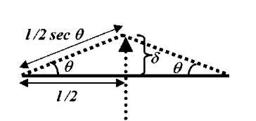
Because of known differences in the electronic response of zigzag and armchair tubes to mechanical deformation, the simulations were performed on a (12,0) zigzag and a (6,6) armchair tube, each consisting of 2400 atoms. The AFM tip was modeled by a 6-layer deep, 15-atom Li needle normal to the (100) direction, terminating in an atomically sharp tip. To simulate AFM tip deformation, the Li needle was initially aimed at the center of a hexagon on the bottom side of the middle part of the tube. The Li needle tip was then displaced by an amount d toward the tube along the needle axis, resulting in a deformation angle 0=tan~ 1(2d/l), l being the unstretched length of the tube. At each end of the tube, a contact region defined by a unit cell plus one atomic ring (a total of 36 and 60 atoms for the armchair and the zigzag tube, respectively) was then fixed, and the whole tube relaxed with the UFF, while constraining the needle atoms as well. The contact region atoms were fixed to simulate an ideal undeformed semiinfinite carbon nanotube lead, and to ensure that all possible contact modes are coupled to the deformed part of the tube. Following the UFF relaxation, a cluster of 132 C atoms for the (6,6) tube, and a cluster of 144 C atoms for the (12,0) tube were cut out from the middle of the tubes. These clusters, referred to below as the QM clusters (plus the 15 Li-tip atoms in tip deformation simulations) were further relaxed with Accelrys’ DFT code DMol3,[62,63,71-73] with the end atoms of the cluster plus the Li-tip atoms fixed at their respective classical positions. To cut down on CPU requirements, the DFT calculations were performed by using the Harris functional[74,75] and the local exchange-correlation potential due to Vosko et al.[76]
Table 1 IP of a (5,5) CNT for various molecules physisorbed on its tip
|
Adsorbate |
Dipole moment (Debye) |
Ionization potential (eV) |
|
H2 |
0.0 |
6.40 |
|
HCl |
1.0 |
6.36 |
|
H2O |
2.0 |
6.30 |
|
HCN |
3.0 |
6.20 |
|
LiH |
5.9 |
6.12 |
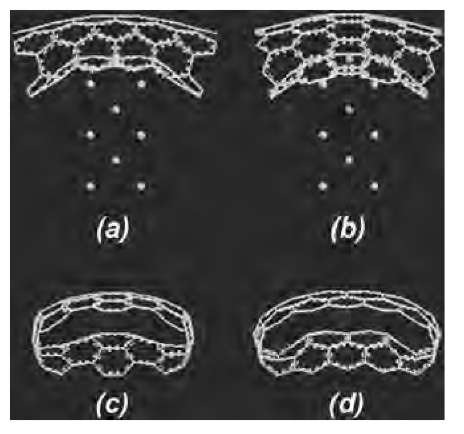
Fig. 4 DMol3-relaxed Li-tip-deformed QM clusters for: (a) the (6,6) armchair (132 C atoms); and (b) the (12,0) zigzag (144 C atoms), in side views. The deformation angle is 25° for both tubes. Panels (c) and (d) are the respective views along the tube length, with the Li tip hidden for clarity.
Fig. 4 displays the tip-deformed QM cluster for (6,6) and (12,0) tubes at the highest deformation angle of 25° considered in these simulations. Even under such large deformations, there is no indication of sp3 bonding, and the structure was very similar to what was observed for a (5,5) tube in a previous work.[77] The absence of sp3 coordination is inferred based on an analysis of nearest-neighbor distances of the atoms with the highest displacements, i.e., the ones closest to the Li tip. Although, for each of these atoms, the three nearest neighbor C—C bonds are stretched to between 1.45 and 1.75 A, the distance of the fourth neighbor, required to induce sp3coordination is greater than 2.2 A for all tubes in our simulations.
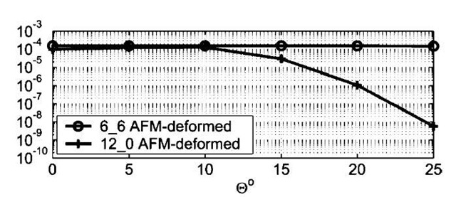
Fig. 5 Computed conductance (in Siemens) of AFM-deformed (6,6) and (12,0) CNTs as a function of deformation angle 8 (in degrees).
Fig. 6 Schematic diagram representing deformation with an AFM tip. The tip-deformed tube undergoes a tensile strain. The deformation angle 8 is related to the tip displacement (d) and nondeformed tube length (l) by 8 = tan~ 1(2d/l).

