ABSTRACT
As scaling continues beyond nano-technology, integrated circuit reliability is gaining increasing concerns in IC (Integrated Circuit) fabrication technology with decreasing transistor gate size, and the impact of trace interconnect failure mechanisms on device performance and reliability will demand much more from integration schemes, interconnect materials, and processes. An optimal low-k dielectric material and their related deposition, pattern lithography, etching and cleaning are required to form dual-damascene interconnect patterns fabrication processes. As technology nodes advance to nanotechnology, metal hard-mask such as TiN is used to gain better etching selectivity and profile controlling to the low-k materials during the pattern etching process. A hard-mask scheme approach of interconnects patterning of wafer fabrication is the ability to transfer patterns into under layers with tightest optimal dimension control. Employing a hard-mask scheme in the fabrication process, successfully achieved lithography patterning, dry etch selectivity in high aspect ratio interconnects comparison with a non hard-mask process were discussed. An optimal planarization treatment of photo-resist, good etch selectivity, a feasible manufacturing integrated process of hard mask dual damascene scheme, optimal profile controlling the critical interconnects and good electrical device performances were studied for tight pitch damascene interconnect architecture.
KEYWORDS: Hard-mask, Wafer Fabrication, Interconnects processes integration.
INTRODUCTION
The increase in integration on an IC leads to a high-density BEOL multi-level interconnection structure which communicates the transistors to the package. The back-end-of line (BEOL) RC delay has gradually become a critical limiting factor in semiconductor circuit performance as a result of the rapid shrinking of critical dimensions of trace width of the semiconductor electronics. Nanotechnology semiconductor wafer manufacturing process defects can often impact product yields, depending on the type, size, and location of the defect, as well as the design and yield sensitivity of the respective semiconductor product devices. The fabrication process defects occurring in a semiconductor device, which involves forming layer patterns on a semiconductor wafer by film patterns formation based on the result of manufacturing processes, thereby reducing the difference in critical dimension of patterns in the patterning process effect, the topology of the wafer, and the difference processing parameter and material. For the implementation of copper and low-k materials into a small pitch damascene interconnect architecture, it is important to understand use of etching and lithography technology to improve the wafer fabrication process technologies.
As design rules continue to shrink, the demand increases for effective inspection tools to detect defects that affect device yields. During BEOL schematic formation, via hole etching, and trench etching are the dominant etching steps to form Cu interconnect layers; these steps are widely applied to manufacture the 90 nm node and beyond. Fabrication defects are one of the principle causes for yield reduction of wafers for IC manufacturers. Defects specification has been a highly problematic aspect of the wafer fabrication industry. The critical applications of anisotropic etching, plasma ashing and cleaning to form precisely controlled profiles of high-aspect-ratio form precise via holes and trenches used in advanced Cu/low-k interconnects in the back end of line (BEOL) are described in detail [1]. Moreover, the investigation of resist pattern collapse with top rounding resist profile was shown in [2]. They found that the pattern size is reduced as the device is more integrated. The resist deformation phenomenon has been a serious problem under 100 nm line width patterns. Because 65nm BEOL trenches etch is apt to suffer the marginal photo-resist issue, it is a big challenge for trench etches process to simultaneously satisfy the requirements for both metal sheet resistance (RJ and connecting resistance (Rc). The advanced process control based on lithographic defect inspection and reduction was proposed [3]. They proposed a methodology based on post lithographic defect inspection, and defective die count analysis was used, which provided effective process monitoring and yield maintenance.
The reliability challenges for copper interconnects were discussed [4]. The three most critical process factors and elements affecting copper interconnect reliability are copper vias and interfaces and the liner coverage. Using a low-k dielectric with a copper interconnect introduces several new challenges to reliability, including dielectric breakdown, temperature cycle, and stability within packages. Effects of width scaling and layout variation on dual damascene copper interconnect electromigration were also demonstrated in [5-6].
By study and optimization of hard mask stacks and etching fabrication; [7] developed dry etch processes for the fabrication of EUV hard mask used for etching in CMOS technology. The controlling surface reactions during etching of SiOCH and organic material model were proposed [8]. With the wide application of low-k dielectric materials at the 90 nm technology node and beyond, the long-term reliability of such materials is rapidly becoming a critical challenge for technology qualification in most important reliability issues during Cu/low-k technology development [9,10].
A method of forming optimal dual damascene process for the BEOL process was proposed [11,12]. To overcome these challenges, accurate and repeatable depth assessment of damascene structures requires the ability to resolve high-aspect-ratio structures in both a high density and isolated structures in the manufacturing process by improving yield.
EXPERIMENTS
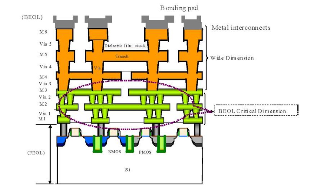
As technology nodes advance to nanotechnology and beyond, IC companies are investigating the use of a metal hard mask in order to gain better etching selectivity to the low-k materials during the dry etching process. A hard mask mechanism approach of fabrication for the modification interconnects fabrication processes of low-k and copper interconnects is used for dual damascene process for critical dimension control to obtain tight profile. When scaling the critical dimensions into nanotechnology, the impact of layout and line edge becomes important. Implementation of Cu and low dielectric constant (low-k) materials in the manufacturing process requires a complete understanding of these process characteristics and the challenges that appear during the hard mask based dual damascene approach. The nanotechnology copper dual damascene architecture was fabricated according to the scheme shown in Fig. 1. Dual-damascene technology in the fabrication of advanced interconnects presents itself as an integration and reliability challenge.
Fig. 1. Semiconductor multilayer interconnects physical structure.
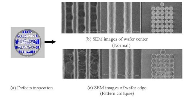
As design rules continue to shrink, the demand increases for effective inspection tools to detect defects that affect device yields. Defect inspection metrology is an integral part of the yield ramp and process monitoring phases of semiconductor manufacturing. Systematic yield losses are process-related problems that can affect all die chips on a wafer. It is important to produce better die chip per wafer by minimizing the cycle time to detect and fix yield problems associated with the advanced process module technology. High aspect ratio structures have been identified as critical structures where there are no known manufacture solutions for defect detection. A serious problem in wafer fabrication is the defects issue during the pattern development process, because it decreases the yield of wafer production. Abnormal patterning phenomena lead to yield loss after the electrical device test and productivity yield losses. Pattern profiles strongly depend on many manufacturing module processes, and can be suppressed by optimization of lithography, cleaning and etch processes. The defects inspection map can be revealed the abnormal pattern profiles, which results in yield loss and abnormal electrical device. In Fig. 2, the defects inspection of the fabrication processes was investigated. Fabrication defects are one of the principle causes for yield reduction of wafers for IC manufacturers. Defects specification has been a highly problematic aspect of the wafer fabrication industry. Interconnect line shorts defects have a high potential of becoming fabrication yield killers for semiconductor manufacturing. It is important for in-line inspections for detecting, classifying and correcting yield limiting defects on all critical manufacturing processes steps.
Fig. 2. Inspection images of comparisons of structure after trench pattern etching.
RESULTS AND DISCUSSION
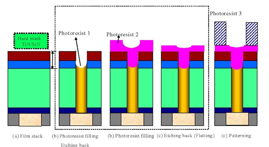
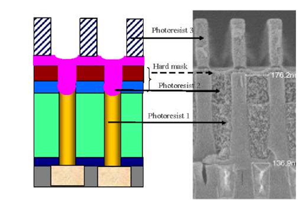
Wafer manufacturing variations can be classified as process systematic and random variations. Process systematic variations are predictable in nature and depending on deterministic factors such as layout structure and surrounding topological environment. A comprehensive evaluation and investigation of the physically relevant causes to develop feasible integrated processes are important for critical dimension interconnect trace. As Fig.3 demonstrated, the hard mask patterning scheme preserves minimizing damage caused by the plasma and strip processes, and reducing the thickness requirement for the underlying barrier film, and enables superior CD and profile control. The comparison of feasible hard mask lithography planarization scheme for dense pattern was also shown in Fig.4. As technology nodes advance to nanotechnology and beyond, IC companies are investigating the use of a metal hard mask such as TiN in order to gain better etching selectivity to the film materials during the dry etching process. Hard mask etching processes have been developed which allowed us to obtain tight profile and CD control. Small amounts of polymer are intentionally left on the sidewalls of trenches and vias during the dry etching process in order to achieve a vertical profile and to protect the low-k materials under the etching mask. As hard mask approach adopted for better CD controlling in manufacturing process, the deposition film stack thickness is also increased. Three steps photo-resist gap fill approach and etching back planarization techniques are the process of increasing the flatness or planarity of the surface of a semiconductor wafer. This treatment method for etching which can increase the metal-to-photo-resist etching selectivity of a metal layer aimed to be etched with respect to photo-resist layers overlaying the metal hard mask layer. Moreover, etching of hard mask presents a challenge, as etching process should find a balance between contradicting requirements of providing sufficient selectivity to photo-resist and avoiding formation of excessive sidewall polymer resulting in CD gain.
Fig. 3. Feasible hard mask planarization integrated processes approach of high aspect ration trench patterning.
Fig. 4. Comparison of feasible hard mask lithography planarization scheme for dense pattern.
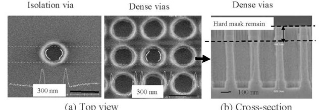
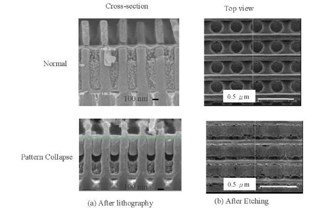
In the comparisons of top SEM view images and cross-section view of dense via chain pattern of Fig.5 illustrates the different critical via chain structure and critical pattern of the improvement for different locations of wafer. Because the extra added hard mask films, consequently the depth of the via is also increased in manufacturing patterning process. The impact of via etching performance of different via chain structure was investigated. Comparing the results from dense and isolation critical via chain schemes shows that this present optimal via profiles. After via etching process, the hard mask remain of dense pattern is enough for the buffer of follow-up processes as: trench etching and chemical mechanical polish. An improved resist etch-back technique using three resist layers also has been developed which offers enhanced planarity over the dielectric film layers process. A photo-resist gap-fill material is used to ensure that the lithography process produces the best profiles and enables critical dimension control. The impact of trench etching on the electrical and reliability performance of different via chain structure was investigated. Fig. 6 illustrates top view SEM image and cross-section of the critical dense via chain developed photo-resist structure. Comparing results of trench developed photo-resist profile, the optimal photo-resist can strongly effect on trench patterning. It was identified that the profile of photo-resist top was severely damaged due to via gap filling attack of the lithography process. To compare lithography photo-resist profile structure for different trench pattern density, the TEM cross section images of trench etching photo-resist profile are illustrated in Fig.7. In order to check the causes of this patterns collapse phenomenon, the profile of photo-resist profile of trench etching is important in process development. For the via-first dual damascene process, a good controlling of photo-resist and via gap filler photo-resist typically used to ensure a lithography process produces the best profiles and critical dimension control and integrates structures having small feature sizes. The via gap filler material treatment may include etching the dielectric layer and the gap-filling material layer to planarize the via gap filler material layer. Therefore, a planarizing bottom photo-resist film and via gap filler material are used to ensure a trench lithography process produces the best profiles and critical dimension control in follow-up etching process.
Fig. 5. Inspections of hard mask remain on different pattern density after via etching.
Fig. 6. Inspections of lithography photoresist profile effects on trench patterning.
Fig. 7. Comparison of lithography photo-resist profile structure for different trench pattern density.
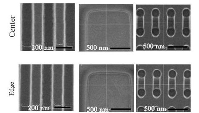
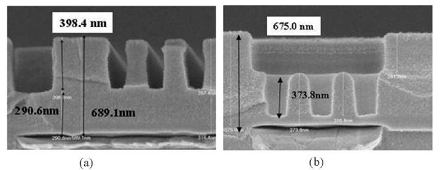
Dry etching processes are commonly used to fabricate vertical sidewall trenches and vias for interconnect dual damascene fabrication processes. The important factor that causes the pattern profile in a dual damascene architecture is the locations and the design pattern density. In comparison the SEM pictures of Fig. 8 show trench etch results by optimal treatment planarization photo-resist gap filling for different dense pattern design. The optimal pattern profile controlling which makes no abnormal pattern even via chain, narrow and wide interconnect trace line for overall wafer. Different lines and via holes with feature sizes down to 100 nm have been realized by in-line process inspection and electrical device verification. The developed etch processes have been successfully applied for high aspect ratio hard mask fabrication. The impact of trench etching on the electrical and reliability performance of different via chain structure was investigated. Fig. 9 illustrates the cross-section of the critical dense via chain structure obtained that was after the trench etching. Comparing results from different critical dense via chain schemes shows that this present optimal integrated processes can also get effective pattern as demonstrated in post trench etch clean of via fist post trench dual damascene process.
Fig. 8. Feasible process inspections on different critical patterns after trench etching.
Fig. 9. Cross-section verification of different via chain pattern after trench etching.
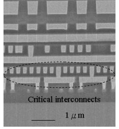
Fig. 10 shows the TEM micrographs of the cross-sectional profiles of Cu dual damascene structure along the silicon substrate / gate transistor / critical interconnects / wide metal interconnects, respectively. The damascene structure of the interconnect chain with the layers identified after copper processes. Consequently, the wafer fabrication integrated process provided the best electrical performance at both dense via chain and isolated via test structures by the present study.
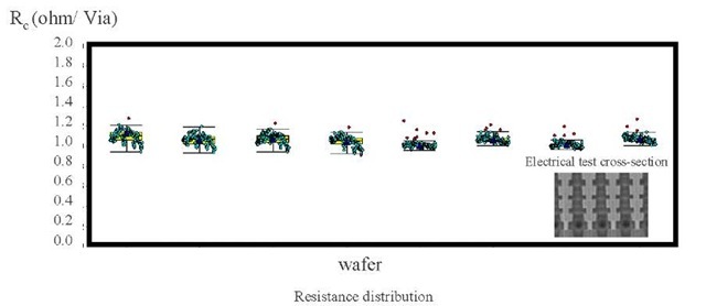
As demonstrated in Fig. 11 (a) and (b), the electrical device test pattern is always used to check the semiconductor process in-line electrical device verification; The drain voltage (VD=1V), for source voltage (VS) and substrate voltage (VSUB); VS=VSUB=0V, and electrical current (Id). The electrical resistance is Rc= VD / Id. The distribution of electrical resistance is tight for optimal integrated process and there are no open electrical test data for optimal integration process. Figs. 11 (b) shows the representative cumulative resistance distribution of the dense via chains associated with the optimal treatment etch processes. The via contact resistance spread of dense via chains were also compared among the different wafer processes.
Fig. 10. TEM inspection of multilayer interconnect scheme.
Fig. 11. Contact resistance of electrical device test of optimal integration process.
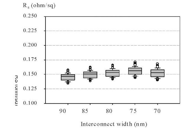
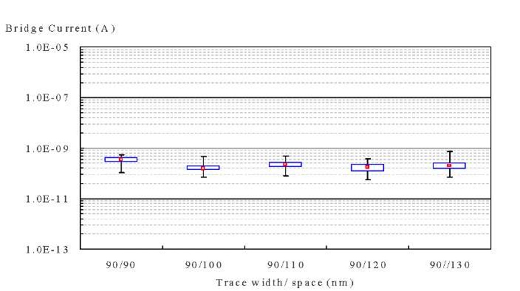
Fig. 12 shows the distributions of sheet resistance measurements of the different interconnect trace width respectively. No significant deterioration of sheet resistance of good trench profiles after the etch process is shown in Fig. 12(b) for comparison. The resistance spread of dense trace lines were also compared among the different pattern width. It is obvious that the wafer fabrication process resulted in the tightest control of resistance spread even 70 nm width. Fig. 13 shows the cumulative distributions of leakage current measurements of the metal bridging-continuity. The line-to-line leakage current of both metal bridging-continuity structures were well controlled. No significant deterioration of line-to-line leakage current is demonstrated. The median leakage current of the trace / space combinations is located below 1.0E-9 A. That means the wafer process provided a better control of the pattern isolation even for 90 nm /90 nm (trace width/ space). Moreover, the integrated wafer fabrication processes resulted in tight distribution of leakage current compared different pattern designs. That means the integrated wafer processes provided a better control of the resistance spread and pattern isolated.
Fig. 12. Interconnect sheet resistance of different width by optimal integration processes.
Fig. 13. Space effects of Interconnect bridge current of optimal integration processes.
CONCLUSIONS
Hard mask etching processes have been developed which allowed us to obtain tight profile and CD control. The impact and improvement of high aspect ratio nanotechnology hard mask dual damascene by integrated manufacturing processes were studied. The effects of integrated fabrication processes on lithography, etching in dual damascene copper interconnects manufacturing processes have been investigated. With the understanding of the complexities involved in copper interconnects and the associated integration processes, a robust reliability is achievable for the new enhancement copper technology.
