Receiver Specifications
Once the requirements of the receiver have been obtained, a number of important steps have to be carried out prior to starting with the receiver design. First of all, the gain, the C/N0, and the linearity of the front-end have to be set to ensure proper performance of the receiver. Moreover, the receiver architecture has to be chosen and all the blocks and external components have to be specified to meet requirements.
Gain The required gain of the RF front-end is defined by the power at the input of the receiver chain and by the input analogue-to-digital converter characteristics. The received input signal at the antenna has to be amplified until the ADC is able to digitalise it. Thus, the gain can be defined as the quotient of the input and output signal as expressed in the following equation.
where![]() is twice the maximum offset of the analogue-to-digital converter estimated to be 50mV [Baghai97] and
is twice the maximum offset of the analogue-to-digital converter estimated to be 50mV [Baghai97] and![]() is the RMS value of the noise over 50Q, which corresponds to -106dBm or 1.12|V (i.e., the threshold noise power at 290K in 6MHz). The system’s voltage gain can now be obtained.
is the RMS value of the noise over 50Q, which corresponds to -106dBm or 1.12|V (i.e., the threshold noise power at 290K in 6MHz). The system’s voltage gain can now be obtained.
Transforming the gain to decibels, it results in:
The fact that the specified gain of 99dB is the minimum required gain for the detection of a signal of -130dBm must be kept in mind. If the gain were higher, lower power signals could be detected, thereby improving the sensitivity of the receiver. Moreover, there would be a surplus of the specified gain if the offset of the ADC were higher than the estimated 50mV. On the other hand, if the ADC had a lower offset, the system gain specification could also be decreased. However, this is usually not a contrasted value for the state-of-the-art technology when the time comes for system analysis.
Once it is defined, system gain should be shared among the blocks that compose the receiver. Before doing so, two critical points that determine final features of the receiver have to be taken into account. First, low-frequency amplifiers are more efficient than high-frequency amplifiers in terms of power consumption. Second, material in which the receiver is fabricated has to be able to isolate output and input in order to avoid oscillation problems caused by positive feedback. As an example, a substrate such as the SiGe process of AMS typically presents isolate levels at 1.6GHz below 40dB, while it is close to 90dB at the 3MHz isolation level. Therefore, splitting gain into different frequencies is required.
C/N0 Degradation Due to the ADC Eq. 2-14 defines the C/N0 without jamming in the baseband. This parameter is directly related to the behaviour of the receiver under the probability of detecting the signal [Kaplan96].
where Sr is the signal power at the input of the system in dBW, Ga is the antenna gain to the satellite in dBic, 10log(£T0) accounts for the thermal noise density in dBW/Hz, NF is the noise figure of the receiver, in dB and L considers the losses in implementation plus the ADC loss in dB. The degradation introduced by the digitalisation of a 1bit ADC can be obtained from [Chang82] and results in 2.2dB.
From the C/N0 required for the system, the noise figure can be calculated by means of the Friis formula or system simulations for a given input signal power, antenna gain, receiver bandwidth, and 1bit ADC from Eq. 2-14. With this relationship, every component of the system can be characterised to make the whole system meet noise specifications.
Interferences Noise is usually defined as the floor of the lowest signal power that can be detected. On the other hand, linearity is defined as the ceiling of the highest signal power the system admits before saturation. The span between these two parameters defines the dynamic range of the receiver. Nevertheless, linearity definition should be slightly redefined in the case of GNSS signals because signal power is never high enough to saturate the system.
Even if the received signal is a low-power narrowband signal in the L1 band, signals from close bands, or even intermodulation products of other signals from other bands, could create a signal in the same band as the target signal. This is why linearity in the first blocks of the system is very important. Those signals will affect the performance of the signal processing, as they will not be filtered in the RF front-end. Therefore, the linearity of the GPS/Galileo receiver is redefined as the limit of the highest interference power that the receiver can handle before it begins to perform incorrectly.
As interferences are unwanted signals, they could be considered noise and therefore reduce the value of C/N0 without distortion. In that case, the equivalent carrier-to-noise power density ratio (C/N0eq) can be defined as in Eq. 2-15, where C/N0 and J/S (the jammer-to-signal power ratio) are related to each other.
where:
■ c/n0 is the carrier power-to-noise without jamming for a 1Hz band expressed as a ratio.
■ j/s is the jammer-to-signal power ratio expressed as a ratio.
■ Rc is the chipping rate of the GPS PRN code (chips/sec).
■ Q is the spread spectrum processing gain adjustment factor (dimensionless).
To obtain the maximum allowed J/S for the receiver, the designer must set the minimum![]() for an acceptable receiver
for an acceptable receiver![]() and the specified
and the specified![]() for the receiver to be designed
for the receiver to be designed![]() which should be equal or lower than the previous one.
which should be equal or lower than the previous one.
The difference between these two values will be the interference margin![]() which is the allowed degradation in the
which is the allowed degradation in the![]() due to interferences and can be calculated by Eq. 2-16.
due to interferences and can be calculated by Eq. 2-16.
Nevertheless, interferences will not only degrade the![]() but also quantification. Thus, even if it has a high enough
but also quantification. Thus, even if it has a high enough![]() the receiver may not work properly due to erroneous digitalisation. Therefore, depending on the quality of the ADC, the blocking level should be higher than the specified value in Eq. 2-16.
the receiver may not work properly due to erroneous digitalisation. Therefore, depending on the quality of the ADC, the blocking level should be higher than the specified value in Eq. 2-16.
In the case of a 1bit ADC, due to the absence of a gain-controlled amplifier (GCA), interferences could cause the signal to cross the zero level in the input of the converter. In this case, the crossing would be generated by the unwanted interference rather than by a combination of random noise and the navigation signal. This would result in both erroneous digitalisation and incorrect localisation.
The maximum allowed degradation for the SNR in the 1bit quantifier by interference is 14dB![]() (Eq. 2-16). This degradation is obtained when J/S is 32dB, which is achieved by an input power signal of -115dBm at the L1 and E1-L1-E2 band frequencies.
(Eq. 2-16). This degradation is obtained when J/S is 32dB, which is achieved by an input power signal of -115dBm at the L1 and E1-L1-E2 band frequencies.
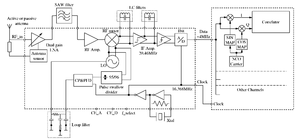
Architecture A multitude of well-known main RF front-end architectures are in existence: heterodyne, direct conversion, intermediate frequency digitalisation, and direct digitalization. For the combined GPS/Galileo front-end, a low-IF architecture can be selected. This architecture, when compared to Zero-IF, is insensitive to DC-offsets and flicker noise. The DC-offset compensation is a severe problem for Zero-IF receivers, as most of the GPS C/A-code signal energy comes from DC. The main drawback of the low-IF architecture is its limited image rejection. This issue can be minimised when the frequency plan of the entire receiver is carefully designed. If the combined GPS/Galileo L1 signal is down-converted to a low IF of 20.42MHz, if the combined GPS/Galileo L1 signal is down-converted to a low IF of 20.42MHz, the rejection of the image signal by the RF SAW filter can be ensured. The obtained image rejection ratio can reach more than 40dB. By sampling the IF signal at 16.638MHz, the A/D converter also down-converts the incoming signal to a second IF of4.092MHz. Signal detection is then performed digitally on a second chip that contains all the digital processing and controlling parts of the receiver. The PLL also allows the choosing of a LO frequency that down-converts the incoming RF signal directly to an IF of 4.092MHz. When this is chosen, the image that lies in the GPS/Galileo L1 band mainly consists of thermal noise. Choosing the gain level within the various blocks of the receiver is always a trade-off. A high-gain LNA will help reduce NF by minimising mixer contribution, but at the expense of higher power consumption in this block. A low-gain LNA may improve linearity and power consumption, but would require a low-noise mixer. Such a mixer would consume a lot of power. In other words, a low-gain LNA combined with a low-noise mixer may not offer a significant advantage in total power consumption over a high-gain LNA combined with a mixer with a higher NF. Therefore, a relatively high-gain receiver configuration has been chosen. Moreover, IF digitali-sation requires few external components and is relatively simple. Thus, the front-end will consist of passive or active antenna, external filters, the LNA, the mixer, the PLL, amplifiers (RF and IF), and the ADC (see Figure 2-14).
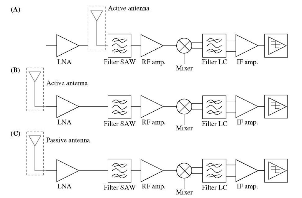
Numerous applications can use a GPS/Galileo receiver. To add felxi-bility to the receiver, three different structures, both with and without an active antenna and the internal LNA have been studied. Figure 2-15 shows all three structures. Structure (A) makes use of an active antenna, avoiding the use of the LNA of the front-end. As the consumption of the LNA is not required, a very low-power front-end can be employed with a separated voltage supply for the LNA. The (B) and (C) structures employ the LNA and its antenna selection sensor, which sets the working mode of the LNA depending on the use of an active or passive antenna. The (B) structure makes use of an active antenna, which means the LNA is set to work in the low-gain mode so as not to saturate the system. Furthermore, higher sensitivity can be achieved by means of the gain of the external antenna. In the (C) structure, a passive antenna is employed and the LNA is set to the high-gain mode, avoiding the power consumption of the antenna and resulting in a low power consumption system.
Figure 2-14 Block diagram of the receiver
Figure 2-15 Receiver block diagram: (A) with active antenna and without the LNA; (B) with active antenna and the LNA; (C) with passive antenna and the LNA
Receiver Chain Specifications The specifications of the components of the proposed front-end are shown in Table 2-5. They have been obtained from the exhaustive system analysis of components and system simulations previously explained in this topic. The supply voltage for the receiver has been defined as 3.3V, the operating temperature range as -30°C ~ +70°C, and the storage temperature as -40°C ~ +85°C.
From system simulations and analyses, gain, noise, linearity, and power consumption have been set to every component of the chain to meet required global specifications. Moreover, input and output impedances have been carefully selected to optimise the system gain and minimise the total noise. Due to the high gain required for the IF amplifier, two stages have been defined. If any change is required during the design stage, system simulations can be redone to reset the specifications for the blocks.
Front-end linearity is not an issue, since the received Galileo and GPS signals are low power and relatively constant. Therefore, the linearity specification is dictated by the required system’s resistance to external interfering signals. The effects of the interferences on the three different structures previously mentioned have been studied for these specifications (see Table 2-5). They have been obtained from system simulations with a two-tone input. In these simulations, the minimum power that generates a third-order intermodulation product at the studied band frequency of -115dBm has been obtained.
TABLE 2-5 Receiver chain specifications
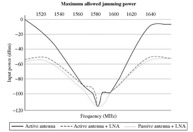
Figure 2-16 Interference blocking for the three receiver architectures under study
Figure 2-16 shows maximum allowed power at the antenna input for interferences in the vicinity. This interference power corresponds with a J/S of 32dB at the L1 and E1-L1-E2 band frequencies. Then the maximum allowed degradation for the SNR in the 1bit quantifier by the interference can be obtained from Eq. 2-15 and Eq. 2-16 giving a Mint erf of 14dB.
To quantify the interference blocking performance of the receiver an example is considered where the point at which the second harmonic of the result of mixing the signals of Inmarsat at 1645MHz and Iridium at 1610MHz reaches 1575MHz. Moreover, GPS antenna patterns experience attenuation when the elevation angle drops below 5°. The attenuation for the horizon line is typically around 15~20dB [Parkinson96]. Therefore, for a transmission power of 37dBm, the GPS/Galileo receiver can be located 50m from emissions without degrading receiver performance.
Frequency Synthesiser Specifications A frequency synthesiser, also known as a phase-locked loop (PLL), is a circuit that synchronises an output signal (generated by an oscillator) with an input reference signal to provide a stable and accurate signal frequency. This synchronisation is done in frequency as well as in phase. When both signals are synchronised, phase error is minimised. As in a control system, the output signal phase remains locked with the reference input signal phase.
Any oscillator signal shows instability in frequency and in amplitude. The target of an oscillator is to generate a signal with a fixed frequency. Frequency instability can be characterised through measurements of either frequency or time. In the time domain, the parameter used to measure instability is jitter noise, while phase noise is used to measure frequency. Moreover, frequency error should be below a certain level of parts per million (ppm). The main parameters used to gauge the performance of the synthesiser are phase noise, lateral band (spurious tones), and lock time. However, lock time is not a critical parameter for GPS/Galileo application due to the absence of different channels.
From the analysis of GPS front-ends, it has been observed that several models have digital outputs of 4.092MHz 1bit signals (i.e., [Atmel ATR0603], [Freescale MRFIC1505], [PHILIPS UAA1570HL], [SONY CXA1951AQ], and [ST STB5610]). This frequency is also suitable for the 6MHz bandwidth of the GPS/Galileo receiver. Therefore, a LO frequency of 1571.328MHz is required, which is mixed to the input frequency of 1575.42MHz. Crystal manufacturers offer a quartz crystal for GPS at a frequency of 16.368MHz. Moreover, this frequency is also employed as a clock for the GPS processor. On the other hand, to improve the frequency planning of the receiver, the down-conversion at the mixer is defined for an IF frequency of 20.42MHz. Therefore, a second LO frequency of 1554.96MHz is required. A 4.092MHz digital output is obtained by the ADC at a sampling frequency of 16.368MHz in the ADC. At the 20.42MHz IF frequency, the image signal is attenuated by the RF SAW filter and a higher rejection to the image signal is achieved. Moreover, mixer noise is also lower because it is filtered by the SAW filter. However, a bandpass filter at 20MHz has to be designed. At 4.092MHz, a low pass filter is sufficient, and efficiency of the IF amplifiers can be improved. Unfortunately, the noise and image signal are not filtered through the SAW filters. The frequencies involved in the PLL are summarized in Table 2-6.
A synthesiser based on integer-N architecture (see Figure 2-17) can be used to obtain the required output frequencies. The integer-N PLL has an output signal frequency N times the reference frequency, N being an integer. The output frequency can be changed by varying the value of N.
TABLE 2-6 Frequencies of the PLL
|
Fref |
16.368MHz |
|
Foutl |
1554.96MHz |
|
Fout2 |
1571.328MHz |
|
ADCout |
4.092MHz |
|
IF1 |
20.42MHz |
|
IF2 |
4.092MHz |
Figure 2-17 Integer-N PLL block diagram
N is 95 in the case of 1571.328MHz and 96 in the case of 1554.96MHz for the reference frequency of 16.368MHz.
The operation of the PLL is as follows: The output signal frequency is divided to compare it to the reference frequency in the phase frequency detector (PFD). Then the result is applied to a loop filter to obtain a control voltage for the VCO to lock the loop that is achieved when the output frequency is the desired one.
The operation conditions for the PLL have been defined by the system analysis. First, phase noise at the PLL has been defined. Three different zones can be distinguished regarding noise source. For frequencies close to the carrier, noise is generated by the crystal; approximately a decade away from the carrier, noise is contributed by PFD. The VCO is the main contributor to the total noise from a distance equal to the bandwidth of the PLL from the carrier frequency[Quemada07], [Simusyn].
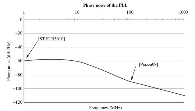
The mask for the phase noise, taken from the analysis, is defined in Figure 2-18. Phase noise of [ST STB5610] has been taken at 1kHz from the carrier and phase noise of [Piazza98] at 100kHz.
Figure 2-18 Phase noise mask
The gain of the![]() is defined as the ratio between frequency and voltage variation. From the two working frequencies, 1554.960MHz and 1571.328MHz, a frequency range of ±0.5 percent is obtained. Component tolerance has to be taken into account as well. Inductor value depends only on geometric values, which is why measured integrated inductor tolerance is around ±1.5 percent[Aguilera03]. Thus, a characterisation of the inductors has to be done prior to the design. Capacitor tolerance is typically ±15 percent due to process variation and ±0.24 percent due to thermal variation[AMS]. Considering the resonance frequency shown in Eq. 2-17, the influence of the capacitor and inductor values on the frequency will be ±7.6 percent and ±0.75 percent, respectively.
is defined as the ratio between frequency and voltage variation. From the two working frequencies, 1554.960MHz and 1571.328MHz, a frequency range of ±0.5 percent is obtained. Component tolerance has to be taken into account as well. Inductor value depends only on geometric values, which is why measured integrated inductor tolerance is around ±1.5 percent[Aguilera03]. Thus, a characterisation of the inductors has to be done prior to the design. Capacitor tolerance is typically ±15 percent due to process variation and ±0.24 percent due to thermal variation[AMS]. Considering the resonance frequency shown in Eq. 2-17, the influence of the capacitor and inductor values on the frequency will be ±7.6 percent and ±0.75 percent, respectively.
Finally, a 1 percent safety margin has been defined to set a PLL specification for the output frequency range of around 10 percent (Eq. 2-18). Therefore, adding tolerance to the working frequencies, the VCO output signal has to oscillate between 1408MHz and 1717MHz.
Once frequency variation is obtained and control voltage is set between 0.5V and 2.8V, VCO gain equals 135MHz/V (Eq. 2-19).
Basic specifications for the PLL are summarised in Table 2-7. The Agilent ADS templates provide an environment to model PLL performance. Open and Closed Loop Simulation of PLL and PLL_Noise Contribution templates are used to characterise the PLL and analyse its noise, respectively.
TABLE 2-7 PLL specifications
|
2ndHarm |
Spurious response, 2nd harmonic |
dBc |
|
|
PN |
Phase noise@ 100kHz |
dBc/Hz |
|
|
Pout |
Output power |
dBm |
|
|
Vcontrol |
Control voltage |
V |
|
|
Current |
Current consumption |
mA |
TABLE 2-8 Input values for the Open and Closed Loop Simulation of PLL template of ADS
|
Fref |
16.368MHz |
|
Foutl |
1554.96MHz |
|
Fout2 |
1571.328MHz |
|
KVCO |
135MHz/V |
|
Kd |
100|iA |
|
40kHz |
With the Open and Closed Loop Simulation of PLL template, a frequency response simulation can be carried out. Nevertheless, lineal models for the VCO, the divider, and the PFD are employed and no phase noise characteristics are considered. The input values for the simulation are shown in Table 2-8. KVCO has already been defined in the previous section. Kd is the current of the charge pump and has been taken from the analysis and PLL simulations that set out to minimise it. Finally, the bandwidth, which is set by the loop filter, is chosen according to the highest value that fulfils the noise and PLL specifications. The absence of different channels in the application offers freedom to choose the loop bandwidth value. The higher it is, the more time it requires to lock the loop and the lower the noise at the output. The bandwidth is set by the loop filter and has an influence on the output noise[Quemada07].
The band attenuation and loop filter components that meet the requirements are obtained from the simulations. The phase margin should be between 30° and 70° as stated in[Wolaver 91]. For a phase margin around 50°, an attenuation of29/30dB and a bandwidth of 40kHz are obtained. The values of the third-order loop filter (see Figure 2-19) have been obtained from these results and are shown in Table 2-9.
Figure 2-20 shows the VCO phase noise contributors and phase noise mask obtained by the PLL_Noise Contribution template for the previously set values. As explained, for frequencies close to the carrier, noise is generated by the crystal.
Figure 2-19 Loop filter circuit scheme
TABLE 2-9 Loop filter values
|
Component |
Value |
Unit |
|
C1 |
659 |
pF |
|
C2 |
3.27 |
nF |
|
C3 |
65 |
pF |
|
R2 |
3.141 |
|
|
R3 |
813 |
Approximately a decade from the carrier, noise is contributed by PFD from a distance equal to the bandwidth of the PLL from the carrier frequency; the VCO is the main contributor to the total noise[Quemada07]. It can be seen that phase noise requirements can be fulfilled, accomplishing the previously defined set of design specifications.
Summary
The front-end has been specified in order to work simultaneously with GPS and Galileo. This has been made possible by a study of the two standards, and the analysis of their requirements and system simulations. Therefore, the next objective, the design of the front-end, can be undertaken.
Figure 2-20 PLL_Noise Contribution template results for the PLL phase noise
![tmpE-200_thumb[2][2] tmpE-200_thumb[2][2]](http://what-when-how.com/wp-content/uploads/2012/02/tmpE200_thumb22_thumb.png)
![tmpE-205_thumb[2][2] tmpE-205_thumb[2][2]](http://what-when-how.com/wp-content/uploads/2012/02/tmpE205_thumb22_thumb.png)
![tmpE-206_thumb[2][2] tmpE-206_thumb[2][2]](http://what-when-how.com/wp-content/uploads/2012/02/tmpE206_thumb22_thumb.png)
![tmpE-208_thumb[2][2] tmpE-208_thumb[2][2]](http://what-when-how.com/wp-content/uploads/2012/02/tmpE208_thumb22_thumb.png)
![tmpE-221_thumb[2][2] tmpE-221_thumb[2][2]](http://what-when-how.com/wp-content/uploads/2012/02/tmpE221_thumb22_thumb.png)


![tmpE-243_thumb[2][2] tmpE-243_thumb[2][2]](http://what-when-how.com/wp-content/uploads/2012/02/tmpE243_thumb22_thumb.png)
![tmpE-245_thumb[2][2] tmpE-245_thumb[2][2]](http://what-when-how.com/wp-content/uploads/2012/02/tmpE245_thumb22_thumb.png)


