Loop Filter
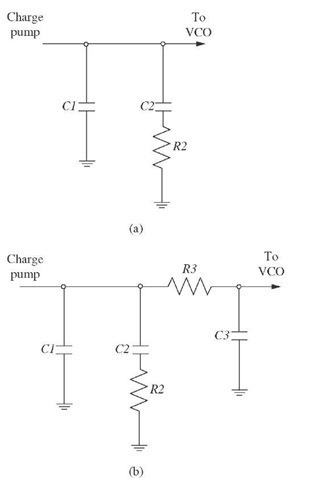
The use of passive filters over active filters in today’s high-performance digital PLL is recommended due to passive filters’ lower noise and complexity. The basic passive filter configuration for a current mode charge pump PLL, such as the one described in the previous sections, is shown in Figure 3-51(a). The loop filter is a complex impedance in parallel with the input capacitance of the VCO. The PFD’s output signals control the charge pump current within the loop filter, which then converts the current into the VCO’s control voltage. An extra-low pass filter section sometimes is needed to provide additional rejection of the reference sidebands, known as spurious. Figure 3-51(b) shows a third-order passive filter where a low-pass filter section (R3 and C3) has been added at the output.
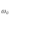
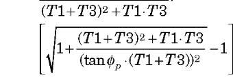
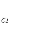
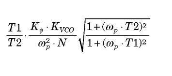
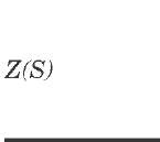
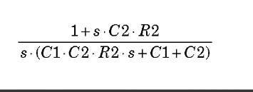
Table 3-15 shows the transfer function![]() of the second- and third-order passive loop filters. The filter component values can be determined from the open loop gain bandwidth
of the second- and third-order passive loop filters. The filter component values can be determined from the open loop gain bandwidth![]() the phase margin
the phase margin![]() the added attenuation from the output low-pass filter section (ATTEN), the Xtal reference frequency
the added attenuation from the output low-pass filter section (ATTEN), the Xtal reference frequency![]() the main divider ratio (N), the phase detector/charge pump constant
the main divider ratio (N), the phase detector/charge pump constant![]() and the voltage-controlled oscillator-tuning voltage constant
and the voltage-controlled oscillator-tuning voltage constant![]() [Kee96].
[Kee96].
Figure 3-51 Passive loop filters: (a) second order and (b) third order
TABLE 3-15 Transfer functions and different equations to determine the filter component values of the second- and third-order passive loop filters
|
Second Order |
Third Order |
||
 |
 |
 |
|
 |
 |
 |
|
 |
 |
 |
|
 |
 |
 |
 |
 |
 |
||
 |
|||
 |
 |
 |
|
 |
 |
 |
|
 |
 |
 |
|
 |
 |
 |
|
 |
 |
 |
|
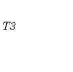
In Table 3-15, T1, T2, and T3 are the time constants that determine the two poles and one zero frequencies, respectively; s is the complex variable;![]() are the frequencies where the open loop gain of the second- and third-order filters respectively are 0dB; and
are the frequencies where the open loop gain of the second- and third-order filters respectively are 0dB; and![]() is the transfer function of the second-order passive filter.
is the transfer function of the second-order passive filter.
TABLE 3-16 Calculated and standard values of the loop filter
|
Parameter |
Simulation |
Standard |
Unit |
|
C1 |
659 |
680 |
pF |
|
C2 |
3.27 |
3.3 |
nF |
|
C3 |
65 |
68 |
pF |
|
R2 |
3.141 |
3 |
Kn |
|
R3 |
813 |
750 |
n |
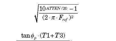
In the design example, a third-order passive loop filter has been selected. Locating the point of minimum phase shift at the unity gain frequency of the open loop response ensures loop stability. The phase relationship between the first pole and the zero also allows easy determination of the loop filter component values, as shown in Table 3-15. The phase margin![]() defined as the difference between 180° and the phase of the open loop transfer function at frequency
defined as the difference between 180° and the phase of the open loop transfer function at frequency![]() has been set to 48°. In this manner, an optimum trade-off between loop stability, attenuation of
has been set to 48°. In this manner, an optimum trade-off between loop stability, attenuation of![]() and loop response has been achieved.
and loop response has been achieved.
Notice that, to attenuate the spurs, the frequency of the additional pole introduced by the output low-pass section is lower than Fref. However, it is higher than the loop bandwidth so as not to compromise loop stability.
Table 3-16 shows the values of loop filter components obtained from the previous equations and the ones matched to the standard values available on the market.
Overall Considerations
This section presents the designed control logic that allows for different working modes by means of three additional control pins. It can switch the entire receiver on or off or switch on only the pierce oscillator and digital buffers of the RF front-end, creating only the clock for the digital IC.
Some considerations about the floor planning of the entire front-end are also presented in this section, which is a key element in the successful completion of the receiver. The location and interconnections of all the blocks have to be carefully designed. The different PADs used in the design, along with their purposes, are also described in this section.
Finally, the necessary external components, such as the antenna, SAW filters, and so on, are listed.
Operation Modes of the Front-End
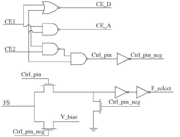
To control the receiver and switch it on and off, three input pins have been defined: two CE (chip enable), CE1 and CE2; and an FS (frequency selection). The logical gates utilised to implement the CE function are shown in Figure 3-52. Four different operation modes can be set using the CE pins (see Table 3-17).
These modes allow the receiver to be switched off (first mode) and the pierce oscillator and the digital output buffers of the RF front-end to be switched on, powering only the clock for the digital IC (third mode). Hence, the RF front-end can be set to stand-by mode when required by the digital IC, minimising power consumption. These modes also allow the complete receiver to be switched on (fourth mode). This is the normal mode of operation. In all the previously mentioned operation modes, the frequency selection pin selects the LO frequency. However, in the second mode of operation, known as test mode, the FS pin allows the current of the different blocks of the entire receiver to be controlled. This way, by means of the intermediate PADs, separate testing of each part of the chip is possible.
Figure 3-52 CE gate diagram
TABLE 3-17 Front-end operation modes
|
CE1 |
CE2 |
FS |
F_select |
CE_D |
CE_A |
V_bias |
Mode |
|
|
0 |
0 |
01 |
0 |
1 |
1 |
1 |
— |
Off |
|
0 |
1 |
V_bias |
0 |
0 |
1 |
V_bias |
Test Mode |
|
|
1 |
0 |
01 |
0 |
1 |
0 |
1 |
— |
Digital On-Analogue Off |
|
1 |
1 |
01 |
0 |
1 |
0 |
0 |
— |
Digital On-Analogue On |
