Pulse Swallow Divider
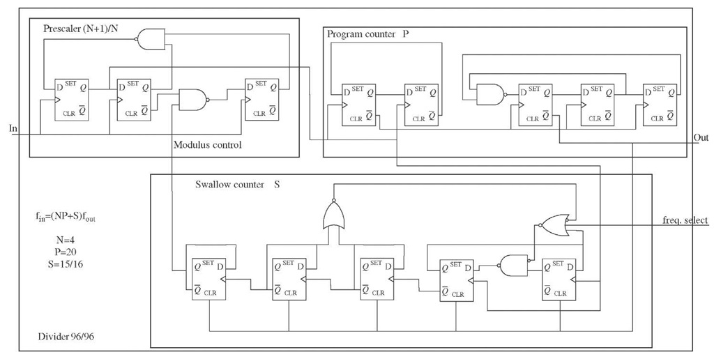
To compare the VCO output signal frequency with the reference Xtal frequency, a divider is required. For the design example, it consists of a dual modulus prescaler (N = 4, (N+1)/N), a program counter (P = 20), and a swallow counter (S = 15/16) (see Figure 3-33). Therefore, from Eq. 3-38 [Razavi97], a division ratio of 95 and 96 is obtained.
where![]() is the output frequency of the VCO and
is the output frequency of the VCO and![]() the signal frequency of the divider output that will be compared using a PFD with the Xtal signal. N is the division ratio of the prescaler, P is the division ratio of the program counter, and S is the division ratio of the swallow counter.
the signal frequency of the divider output that will be compared using a PFD with the Xtal signal. N is the division ratio of the prescaler, P is the division ratio of the program counter, and S is the division ratio of the swallow counter.
Figure 3-33 shows the architecture of the pulse swallow divider. Due to the high frequency of the incoming signal (1.575GHz), a prescaler has been implemented using emitter-coupled logic (ECL). The program counter and the swallow counter work at frequencies between 310MHz and 393MHz. Thus, CMOS logic has been used to minimise power consumption. Moreover, a comparator is required as an interface to convert the signal level from ECL to CMOS logic.
To work properly, signal delay through the different gates must be smaller than the duration of the incoming signal. Otherwise, pulses might be lost and a different division ratio will be obtained. Therefore, gates have been carefully designed to minimise delays, particularly in the swallow counter, which sets the prescaler divider ratio. The output frequency (16.368MHz) is compared to the reference frequency by the phase frequency detector.
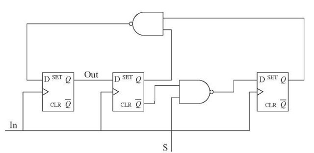
Prescaler The high-frequency prescaler consists of three D flip-flops and two NAND gates (see Figure 3-34). The division ratio is controlled by a counter through the control modulus input (S) coming from the swallow counter. If the modulus control is "high," the division ratio will be 5. On the other hand, if the modulus control is "low," the division ratio will be 4.
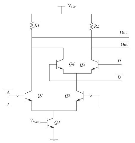
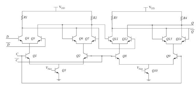
Although requiring higher current, ECL logic has been chosen due to its high operation speed, which allows it to perform correctly at the desired frequencies of 1554.96MHz and 1571.328MHz. Required D flip-flops and NAND gates have been designed at transistor level with a differential architecture to load the output of the VCO differentially.
Figure 3-33 Pulse swallow divider block diagram
Figure 3-34 Diagram of the prescaler
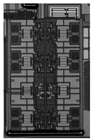
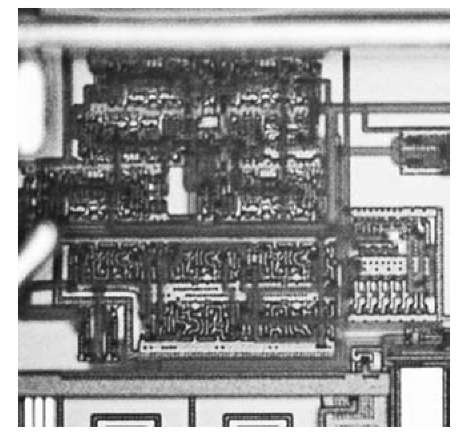
These standard ECL architectures are shown in Figure 3-35 and Figure 3-36. The implemented D flip-flop consists of two differential master-slave latches. The operation of the flip-flop has two steps: In the first clock pulse, input data is stored; in the second clock pulse, the stored data is set as the output. Figure 3-37 shows the microphotograph of the layout of the prescaler.
Figure 3-35 NAND circuit schematic
Figure 3-36 D flip-flop circuit schematic
Figure 3-37 Microphotograph of the prescaler
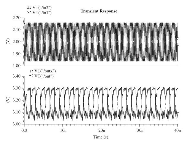
Table 3-13 shows the post-layout results for the two possible settings of the prescaler in regards to the output frequency and the current consumption. Figure 3-38 shows the input and output signals of the prescaler. The input signal is a sinusoidal signal at a frequency of 1.575GHz and the output signal frequency is divided either by 4 or 5, depending on the selection pin. The simulation results have revealed that the prescaler is very sensitive to power supply and ground noise. Therefore, non-ideal ground and a noisy power supply have been included at the simulation stage, and large coupling capacitors have been placed between VDD and GND. Moreover, the delays have been minimised with short connection paths and small area components to minimise the parasitic capacitances.
Comparator To convert the output ECL signal from the prescaler to a CMOS logic signal for the digital divider input, an interface is required. The output frequency for the prescaler is around 350MHz, with an amplitude of 250mV peak to peak and a DC voltage of 3.17V (see Figure 3-38). The CMOS logic-required signal is a square signal centred in 1.65V with a 3.3V peak-to-peak amplitude voltage.
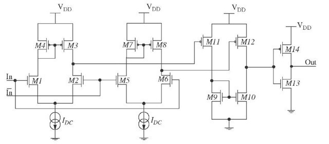
The signal conversion is carried out by the differential comparator shown in Figure 3-39. The resulting consumption of the component is less than 1mA.
TABLE 3-13 Post-layout analysis results for the prescaler
|
S |
Fin |
Fout |
Current Consumption |
|
0V |
1.6GHz |
400MHz |
|
|
3.3V |
1.6GHz |
320MHz |
Figure 3-38 Input (top) and output (bottom) signals of the prescaler
Figure 3-39 Comparator schematic
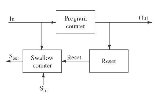
Digital Divider The digital divider consists of a program counter, a swallow counter, and a reset. The working frequency range of the input signals is between 315MHz and 393MHz. The output frequency is 16.368MHz and is compared with the Xtal reference frequency. The block diagram is shown in Figure 3-40.
Figure 3-40 Block diagram of the digital divider
Figure 3-41 Layout of the digital divider
The current consumption of the digital divider, depending on the division ratio, is 852|A for S = 3 V and 883|jA for S = 0 V. Figure 3-41 shows the layout with an area of 74x100pm2. Special attention has been paid to the swallow counter design to minimise gate delays, as an erroneous output signal frequency could result in a divider malfunction. Therefore, a careful layout has been performed to connect different gates to minimise parasitic capacitances caused by signal tracks.
