Digital Circuits and Memory Devices
The reader might legitimately wonder at this point how transistors are used in computers and similar devices. Even though this topic sidetracks the flow of our presentation somewhat, a few introductory remarks on switching devices, information processing, and information storage may nevertheless be of interest. We need to start with the recognition that electronic data-processing systems use binary digits, i.e., zeros and ones as carriers for information. As an example, the numeral sequence "0010" means in the binary system the decimal number "two," whereas 0101 represents the decimal number 5. The first digit at the right of a binary number represents 20, the next digits represent, consecutively, 21, 22, 23, etc. A binary digit, or a bit, is the smallest possible piece of information. (A group of related bits, e.g., 8 bits for word processing, is called a byte.) A "zero" in the present context means that the electric current is off, whereas a "one" means that the current is on. So much about preliminaries.
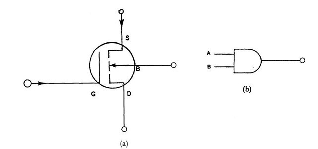
Let us begin with an "AND" device. We inspect the normally-off MOSFET in Fig. 8.29 and see that a voltage on the drain terminal is only obtained if we apply voltages simultaneously to the source and the gate terminals. In other words, a source voltage and a gate voltage cause a voltage on the drain terminal, see Fig. 8.39(a). The circuit resembles a gate in a fence and is therefore called an AND gate. The circuit symbol for an AND gate is depicted in Fig. 8.39(b).
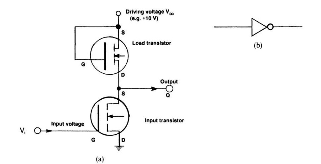
Next, we discuss the inverter circuit. It consists of two normally-off MOS transistors which are wired in series (Fig. 8.40). The upper or load transistor (whose channel is made long and narrow to restrict the current flow) is always kept "on" by connecting the driving voltage to its gate.
Figure 8.39. (a) AND gate and (b) circuit symbol for an AND gate.
Figure 8.40. Inverter made of two "normally-off" (n-channel, enhancement-type) MOSFETs (NOT gate). (a) circuit; (b) symbol in wiring diagram. (VDD means "Drain power supply voltage".) The load transistor may be replaced by a (poly-silicon) resistor or an enhancement-type p-channel MOSFET.
If a high enough voltage is simultaneously applied to the gate of the lower or input transistor, then this lower MOSFET likewise becomes conducting and the driving voltage drains through both transistors into the ground. As a consequence, the output voltage at terminal Q is nearly zero. Thus, the inverter circuit inverts a "one" signal on the input terminal into a "zero" signal on the output terminal (and vice versa). The circuit symbol for an inverter (or "NOT gate") is shown in Fig. 8.40(b).
We have just mentioned that the current through the load transistor is relatively small due to its special design. Still, an inverter which essentially does not consume any power (except during switching) would be even more desirable. This is accomplished by CMOS technology, i.e., by using an enhancement-type p-channel MOSFET as a load transistor, and an enhancement-type n-channel MOSFET as an input transistor. Unless the circuit is switching, one MOSFET is always off (not conducting current) whereas the other is on. Since the two MOSFETs are connected in series similarly as in Fig. 8.40, little power (except due to leakage current) is consumed. It is left to the reader to draw up and discuss the appropriate circuit diagram. (See Problem 18.)
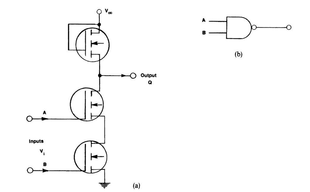
The next logic device that we discuss is a "NAND" circuit. It consists of a load MOSFET, wired in series with two (or more) input transistors. All MOSFETs shown in Fig. 8.41 are of the "normally-off" type. Assume that high enough voltages are applied to the gates of both input transistors to make them conducting.
Figure 8.41. (a) NAND gate and (b) circuit symbol for a NAND digital function.
Thus, the output terminal Q is connected to ground, i.e., the output voltage is almost zero. Since input voltages on the gates of the A and the B transistors inverts the input signal from "one" to "zero," we call the present logic building block an "AND" gate combined with a "NOT circuit" and term the entire digital function "NOT-AND" or a "NAND" gate for short. The reader may convince himself that the output is always "one" when at least one of the input voltages is "zero." On the other hand, if both inputs are "one," the output is "zero."
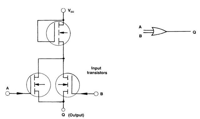
In an "OR" gate (Fig. 8.42) the output voltage Q is "one" when either A or B (or both) possess a voltage. Otherwise Q is "zero."
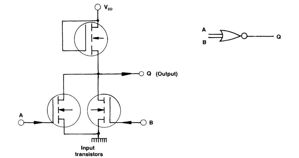
Finally, in a "NOR" circuit, the input transistors are again wired in parallel (Fig. 8.43). Applying high enough gate voltages to one or all of them causes the output voltage to be "zero." The circuit is appropriately called "NOT-OR" or "NOR." Evidently, the output voltage is only "one" if all input voltages are "zero."
In short, the five basic building blocks that are obtained by properly circuiting one or more transistors are AND, NAND, OR, NOR, and NOT.
We are ultimately interested in knowing how a memory device works, i.e., we are interested in a unit made of transistors which can store information. For comparison, a toggle switch that turns a light on or off can be considered to be a digital information storage device. It can be flipped on and then flipped off to change the content of its information. Appropriately, the device that we are going to discuss is called a flip-flop. Let us assume that a flip-flop has a built-in latch to prevent the accidental change of information.
Figure 8.42. OR logic circuit with circuit symbol.
Figure 8.43. NOR logic circuit with circuit symbol.
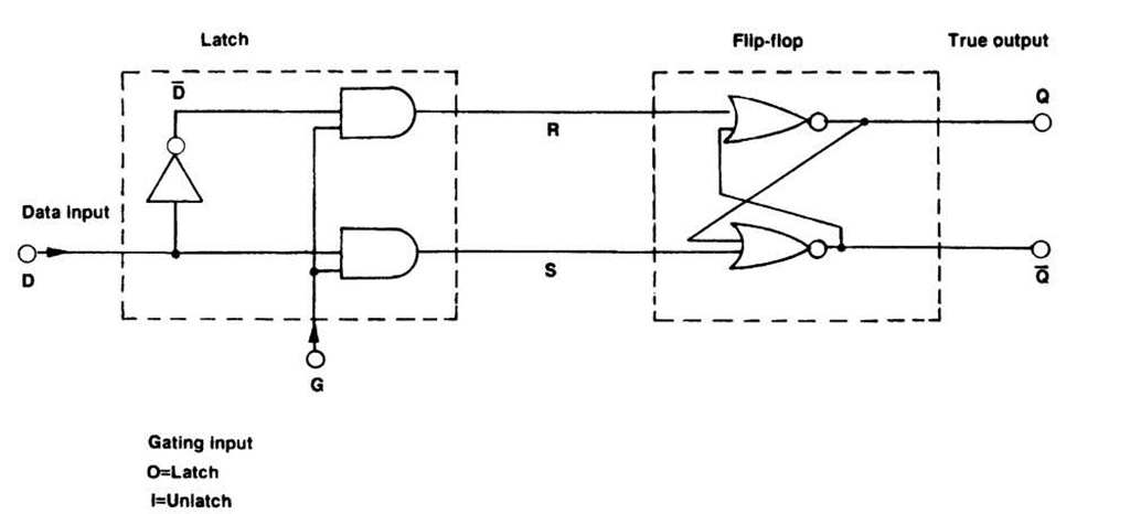
Figure 8.44. SRAM memory device called R-S flip-flop with latch. (The bar on a letter signifies the complement information).
This is done electronically by combining a NOT gate with two AND gates, as shown in the left part of Fig. 8.44. (The output of an AND gate is zero as long as one of the inputs is zero!) It is left to the reader to figure out the various combinations. As an example, if the gate is unlatched (1) and the data input is 1, we obtain "zero" on the R terminal and "one" on the S terminal.
The flip-flop on the right part of Fig. 8.44 consists of two NOR gates which are cross-coupled. (Remember that the output of a NOR is always zero when at least one input is one, and it is one when both inputs are zero.) The above example with R = 0 and S = 1 yields a "one" at the output terminal Q (and a "zero" at the complement output Q), i.e., D and Q are identical. The information that is momentarily fed to the D terminal and into the system is permanently stored in the flip-flop even when the wires R and S are cut off. The cross-coupling keeps the two NOR gates mutually in the same state at least as long as a driving voltage remains on the devices. In short, one bit of information has been stored.
Let us now latch the gating network, i.e., let G be "zero." Whatever option the data input D will assume in this case, the output Q will always be "one," as the reader should verify. In other words, the latching prevents an accidental change of the stored information. On the other hand, latching and unlatching by itself does not change the information content of the flip-flop either!
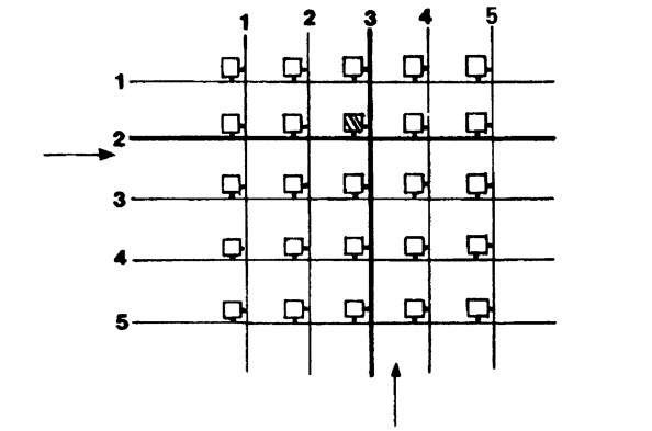
The device described above is called a static random-access memory or, in short, an "S-RAM", because the information remains permanently in the storage unit. The memory cell shown in Fig. 8.44 can evidently store only one bit of information. Let us now imagine a two-dimensional array of these storage elements, connected in a number of horizontal and vertical lines (Fig. 8.45). A designated memory element, being located at the cross point of a specific row and a specific column wire, can then be exclusively addressed by sending an electrical impulse through both wires simultaneously. One of these wires operates on the gating input (Fig. 8.44), the other one activates the data input. As we have discussed above, only a simultaneous activation of both input wires can change the information content of a flip-flop. An array of 32 columns and 32 rows of memory elements constitutes 1024 bits of information storage, or one kilobit. (Yes, a K bit is not 1,000 bits.)
Figure 8.45. Schematic representation of a two-dimensional memory addressing system. By activating the #2 row wire and the #3 column wire, the content of the cross-hatched memory element (situated at their intersection) can be changed.
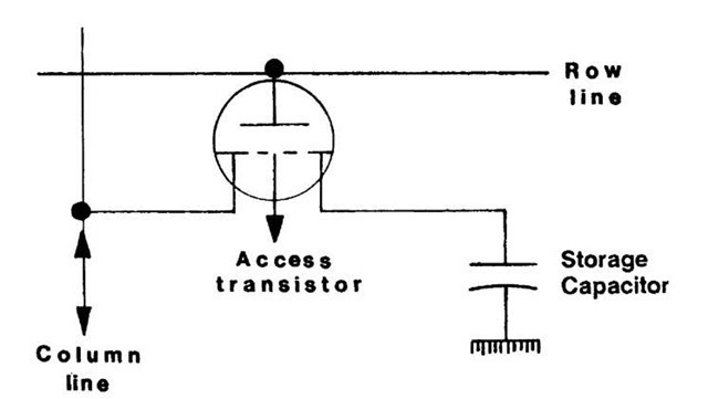
In order to reduce the area on a chip and the power consumption of a storage device, a memory cell different from the above-introduced flip-flop is frequently used. It is called the one-transistor dynamic random-access memory (DRAM, pronounced D-RAM). The information is stored in a capacitor, which can be accessed through an enhancement-type transistor (Fig. 8.46). Only concomitant voltages on gate and source allow access to the capacitor. Since the stored charge in a capacitor leaks out in a few milliseconds, the information has to be "refreshed" every 2 milliseconds by means of refresh circuits. No voltage on the capacitor is used as a "zero," whereas a certain voltage on the capacitor represents the "one" logic.
The 256 Megabit chip combines a multitude of these or similar building blocks through ultra-large-scale integration (ULSI) on one piece of silicon the size of a finger nail.
The memory devices discussed so far are of the "volatile" type, i.e., they lose their stored information once the electric power of the computer is interrupted. In nonvolatile memories, such as the read-only memory (ROM), information is permanently stored in the device. Let us consider, for example, the MOSFET depicted in Fig. 8.29. Assume that the connection to the gate has been permanently interrupted during fabrication. Then the transistor will never transmit current from source to drain. Thus, a "zero" is permanently stored without the necessity to maintain a driving voltage. If, on the other hand, the path to the gate is left intact, the MOSFET can be addressed and current between source and drain may flow, which constitutes a "one." The stored information can be read, but it cannot be altered.
In the programmable read-only memory (PROM) the information may be written by the user, for example, by blowing selected fuse links to the gate. As above, the alteration is permanent and the information can be read only.
Figure 8.46. One-transistor dynamic random-access memory (DRAM). The information flows in and out through the column line.
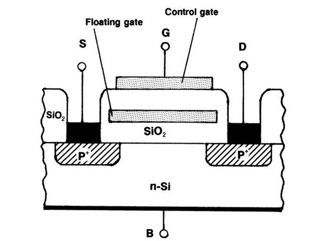
Figure 8.47. Electrically erasable-programmable read-only memory device (EEPROM), also called stacked-gate avalanche-injected MOS (SAMOS), or, with some modifications, flash memory device.
The erasable-programmable read-only memory (EPROM) allows the user to program the device as well as erase the stored information. An EPROM contains a "floating gate," i.e., a gate (consisting of heavily doped polysilicon) which is completely imbedded in SiO2, see Fig. 8.47. For programming, the drain-substrate junction is strongly reverse biased until avalanche-breakdown sets in (see Fig. 8.20), and electrons are injected from the drain region into the SiO2 layer. Alternatively, a large negative voltage (^25 V) between a second gate, the control gate, and the substrate allows some electrons to cross the insulator, thus negatively and permanently charging the floating gate. The oxide thickness is on the order of 100 nm, which assures a charge retention time of about 100 years. A permanent charge on the floating gate constitutes a "1"; no charge represents the zero state (see below). Exposure of the EPROM to ultraviolet light or X-rays through a window (not shown in Fig. 8.47) increases the conductivity of the insulator and allows the charge to leak out of the floating gate, thus erasing any stored information.
For electrical erasure, a large positive voltage can be applied to the control gate which removes the stored charge from the floating gate. This returns the "electrically erasable-programmable ROM" (EEPROM) to the zero state. Alternately, electrical erasure can be performed by applying a "large" positive voltage to the source, which also pulls charge from the floating gate.
The "flash memory" device applies this erasure and writing method. It utilizes a thinner (10 nm) and higher-quality oxide below the floating gate which improves efficiency and reliability. Specifically, the floating gate can be negatively charged ("filled with electrons"), as mentioned above, by a strong, reverse bias pulse between the drain/substrate junctions sufficient to cause an avalanche-breakdown so that electrons are injected from the drain region into the SiO2 layer. Now, a negatively charged floating gate attracts positive charge carriers from the underlying n-substrate (however few they may be) into the channel between source and drain and repels negative charge carriers away from the channel. This allows a hole-current flow between source and drain, see Fig. 8.47. On the other hand, a large and short positive voltage pulse on the control gate removes the electrons from the floating gate so that no positive charge carriers are present between source and drain and no hole-current can flow. These represent the "1" and the "0" states respectively.
Flash memories can be found among others in smartphones, MP3 players, video players, digital cameras, USB memory sticks, global positioning systems, and some computers (particularly laptops). Their main advantages are that they retain information without requiring constant power, they provide higher storage capacity than other same-size silicon-based devices (256 GB as of 2010), their access times are about 20 times faster than for floppy disks, they are small, withstand high pressures and extreme temperatures, have no moving parts (as in magnetic or optical disks), and operate quietly. The main drawback of flash memories is that they eventually degrade as a consequence of a large number (10,000 to 1,00,000 write/ erase cycles), that is, due to voltage bursts across the cells. Furthermore, the floating gate in flash memories leaks electrons over extended time periods and may be corrupted by high energy radiation (e.g. X-rays and g-rays) yielding to about 10 years of data retention time.
Two different logic technologies have been developed: The NOR logic (see Fig. 8.43) can retrieve as little as one single byte. This is achieved by writing and reading data on specific memory sites, thus allowing random access to any memory location. NOR flash memories have relatively "long" erase and write times (tens of ms). They are commonly used in cell phone operating systems and in BIOS start-up programs for computers.
In contrast, NAND logic writes sequentially (see Fig. 8.41), handles the data in small blocks (hundreds to thousands of bits), has ten times the lifetime of NOR flash devices, and reads faster than it writes. NAND-based devices are less expensive than NOR memories and have shorter erase and writing times. Typically, a block of data is written in about 1 ms. NAND devices are quite suitable for massive data storage, such as memory sticks, and other applications where large amount of data need frequent updates.
It is estimated that industry presently (2010) sells about 22 billion dollars worth of flash memories, accounting for about 34% of the semiconductor memory market, and 8% of the overall semiconductor market. These numbers may increase once flash memories become serious competitors for magnetic hard drives.
Another non-volatile memory device is the phase-change random access memory (PRAM). It utilizes chalcogenide glass/ceramic (which contains chalcogen elements, such as selenium and/or tellurium). Most of the present PRAMs are composed of Ge2Sb2Te5. They can be switched from crystalline to amorphous states by application of heat, generated by a short (ns), high voltage pulse, (called reset pulse) which causes localized melting above 600°C, followed by quenching at109 K/s). Local reheating above the recrystallization temperature (but below the glass transition temperature, Tg) applying a longer and lower voltage pulse (set pulse) transforms these materials back into the energetically favorable, crystallized state, erasing the stored information. Switching times of approximately 5 ns have been reported. The amorphous state has a high resistance and represents a binary "0", whereas the low resistant, crystalline state represents a "1". The crystalline state of chalcogenide glasses are distinguished by an octahedral-like arrangement of atoms, often accompanied by strong lattice distortions and large vacancy concentrations.
The main advantages of PRAMs is their slower rate of degradation during use (1 to 100 million write cycles, with lifetimes estimated up to 300 years), their lack of vulnerability against high-energetic radiation, high chemical stability, and high water resistance. Disadvantages are their sensitivity to heat, particularly due to soldering, and relatively higher power consumption during switching.
Phase-change materials are also in use in rewritable optical data storage media, such as in DVD-RW (digital versatile disks-rewritable), DVD+RW, and CD-RW (compact disks-rewritable) where short (ns) laser pulses change the phase states. We shall revisit this application in Section 13.10.
It should be mentioned in closing that magnetic storage devices are discussed in Section 17.4. Optical storage devices are explained in Section 13.10.
