Band Structure
We have seen in topic 7 that metals are characterized by partially filled valence bands and that the electrons in these bands give rise to electrical conduction. On the other hand, the valence bands of insulators are completely filled with electrons. Semiconductors, finally, represent in some respect a position between metals and insulators. We mentioned in topic 6 that semiconductors have, at low temperatures, a completely filled valence band and a narrow gap between this and the next higher, unfilled band. The latter one is called the conduction band. We discuss this now in more detail.
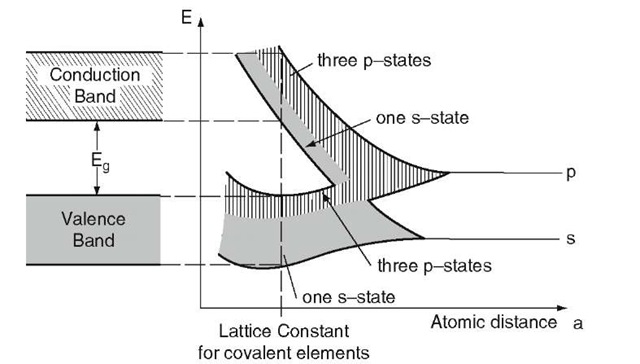
Because of band overlapping, the valence as well as the conduction bands of semiconductors consist of mixed (hybrid) s- and p-states. The eight highest s + p states (two s- and six p-states)8 split into two separate (s + p) bands,8 each of which consists of one s- and three p-states (see Fig. 8.1). The lower s-state can accommodate one electron per atom, whereas the three lower p-states can accommodate three electrons per atom. The valence band can, therefore, accommodate 4Na electrons. (The same is true for the conduction band.) Because germanium and silicon possess four valence electrons per atom (group IV of the Periodic Table), the valence band is completely filled with electrons and the conduction band remains empty.
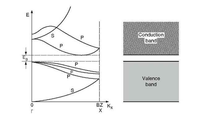
A deeper understanding of this can be gained from Fig. 8.2, which depicts part of a calculated band structure for silicon. Consider at first that electrons are "filled" into these bands like water being poured into a vessel.
Figure 8.1. Sharp energy levels, widening into bands, and band overlapping with decreasing atomic distance for covalent elements. (Compare with Fig. 4.14.)
Figure 8.2. Schematic band structure of silicon in the kx (or X) direction (plotted in the reduced zone scheme). The separation of the two highest p-states in the valence band is strongly exaggerated. Compare with the complete band structure of Fig. 5.23.
Then, of course, the lowest s-state will be occupied first. Since no energy gap exists between the top of the s-state and the next higher p-state, additional electrons will immediately start to occupy the p-states. This process proceeds until all three lower p-states are filled. All of the 4Na electrons of the semiconductor are accommodated now. Note that no higher energy band touches the p-states of the valence band. Thus, an energy gap exists between the filled valence and the empty conduction band. (As was shown in Fig. 5.23, the bands in different directions in k-space usually have different shapes so that a complete assessment can only be made by inspecting the entire band structure.)
Table 8.1. Gap Energies for Some Group IV Elements at 0 K (see also topic 4).
|
Element |
Eg [eV] |
|
C (diamond) |
5.48 |
|
Si |
1.17 |
|
Ge |
0.74 |
|
Sn (gray) |
0.08 |
All materials which have bonds characterized by electron sharing (cova-lent bonds) have in common the above-mentioned hybrid bands (Fig. 8.1). An important difference is the magnitude of the gap energy, Eg, between the conduction band and the valence band. As can be seen from Table 8.1, the gap energies for group IV elements decrease with increasing atomic number. Diamond, for example, has a gap energy of 5.48 eV and is, therefore, an insulator (at least at and below room temperature) whereas the Eg for silicon and germanium is around 1 eV. Gray tin, finally, has an energy gap of only 0.08 eV. (It should be noted in passing that the utilization of diamond as an extrinsic semiconductor has been demonstrated.)
The gap energy is slightly temperature dependent according to the empirical equation
where Eg0 is the band gap energy at T = 0K, X ~ 5 x 10⁻⁴ eV/K, and 0D is the Debye temperature (see Table 19.2). It is noted that Eg becomes smaller with increasing temperature. For example, the temperature dependence of Eg for Si is -2.4 x 10⁻⁴ eV/K (see topic 4).
Intrinsic Semiconductors
Semiconductors become conducting at elevated temperatures. In an intrinsic semiconductor, the conduction mechanism is predominated by the properties of the pure crystal. In order for a semiconductor to become conducting, electrons have to be excited from the valence band into the conduction band where they can be accelerated by an external electric field. Likewise, the electron holes which are left behind in the valence band contribute to the conduction. They migrate in the opposite direction to the electrons. The energy for the excitation of the electrons from the valence band into the conduction band stems usually from thermal energy. The electrons are transferred from one band into the next by interband transitions.
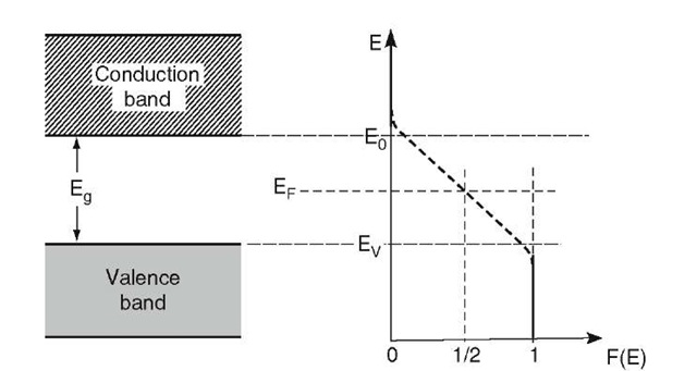
We turn now to a discussion of the Fermi energy in semiconductors. We learned in Section 6.2 that the Fermi energy is that energy for which the Fermi distribution function equals 1 (It is advisable to keep only this "definition" of the Fermi energy in mind. Any other definition which might give a correct understanding for metals could cause confusion for semiconductors!) The probability that any state in the valence band of an intrinsic semiconductor at T = 0 K is occupied by electrons is 100%, i.e., F(E) = 1 for E < Ev (Fig. 8.3). At higher temperatures, however, some of the electrons close to the top of the valence band have been excited into the conduction band. As a consequence, the probability function F(E) is slightly reduced at the top of the valence band for T > 0 K.
On the other hand, no electrons are found at T = 0 K in the conduction band. Thus, the Fermi distribution function for E > E0 must be zero. Again, for higher temperatures, a small deviation from F(E) = 0 near the bottom of the conduction band is expected (Fig. 8.3). The connection between the two branches of the F(E) curve just discussed is marked with a dashed line in Fig. 8.3. This connecting line does not imply that electrons can be found in the forbidden band since F(E) is merely the probability of occupancy of an available energy state. (A detailed calculation provides a slightly modified F(E) curve whose vertical branches extend further into the forbidden band.)
Our discussion leads to the conclusion that the Fermi energy, EF (i.e., that energy where F(E) = 2), is located in the center of the forbidden band. In other words, for intrinsic semiconductors we find EF = — Eg/2 when the zero point of the Energy scale is placed at the bottom of the conduction band.
We may also argue somewhat differently: For T > 0 K the same amount of current carriers can be found in the valence as well as in the conduction band. Thus, the average Fermi energy has to be halfway between these bands. A simple calculation confirms this statement. (Problem 3 in this topic should be worked at this point to deepen the understanding.) We implied in our consideration that the effective masses of electrons and holes are alike (which is not the case; see topic 4).
Figure 8.3. Schematic Fermi distribution function and Fermi energy for an intrinsic semiconductor for T > 0 K. The "smearing out" of the Fermi distribution function at E0 and EV is exaggerated. For reasons of convenience, the zero point of the energy scale is placed at the bottom of the conduction band.
Of special interest to us is the number of electrons in the conduction band. From the discussion carried out above, we immediately suspect that a large number of electrons can be found in the conduction band if Eg is small and, in addition, if the temperature is high. In other words, we suspect that the number of electrons in the conduction band is a function of Eg and T. A detailed calculation, which we will carry out now, verifies this suspicion.
In Section 6.4 we defined N* to be the number of electrons that have an energy equal to or smaller than a given energy, En. For an energy interval between E and E + dE, we obtained (6.9),
where
was called the population density (6.7) and
is the density of states (6.5). In our particular case, the Fermi distribution function, F(E), can be approximated by
because E — EF is about 0.5 eV and kBT at room temperature is of the order of 10—2 eV. Therefore, the exponential factor is large compared to 1 (Boltzmann tail). We integrate over all available electrons that have energies larger than the energy at the bottom of the conduction band (E = 0), and obtain, with (8.2), (8.4), and (8.5),9
or
Integration9 yields
Introducing![]() (see above) and the effective mass
(see above) and the effective mass![]() we then obtain, for the number of conduction-band electrons per unit volume, Ne = N*/V,
we then obtain, for the number of conduction-band electrons per unit volume, Ne = N*/V,
The constant factor
has the value
Thus, we can write for (8.8)
We see from (8.9) that the number of electrons in the conduction band per cm3 is a function of the energy gap and the temperature, as expected. We further notice that the contribution of a temperature increase to Ne resides mostly in the exponential term and only to a lesser extent in the term T3=2. A numerical evaluation of (8.9) tells us that the number of electrons per cubic centimeter in silicon at room temperature is about 109 (see Problem 1). In other words, at room temperature, only one in every 1013 atoms contributes an electron to the conduction. This explains the poor conduction of Si, see Fig. 7.1. We shall see in the next section that in extrinsic semiconductors many more electrons can be found in the conduction band.
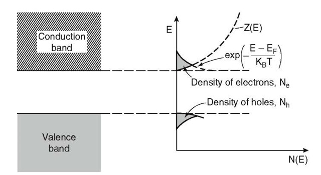
The electron and hole density is shown in Fig. 8.4 for an intrinsic semiconductor. The number of electrons is given by the area enclosed by the Z(E) curve and F(E) = exp[—(E — EF)/kBT] (8.6).
As implied before, the number of electrons in the conduction band must equal the number of holes in the valence band. This means that an identical equation to (8.8) can be written for the holes if we assume![]() which is not strictly true.11 (An additional term, which is usually neglected, modifies EF slightly.)
which is not strictly true.11 (An additional term, which is usually neglected, modifies EF slightly.)
Figure 8.4. Density of electrons (Ne) and holes (Nh) for an intrinsic semiconductor.
The conductivity11 of an intrinsic semiconductor is not determined by the number of electrons and holes alone. The mobility11, m, of the current carriers,
i.e., their (drift) velocity per unit electric field, also contributes its share to the conductivity, s. An expression for the conductivity is found by combining (7.2),
and (7.4),
with (8.10), which yields
Taking both electrons and holes into consideration we can write
where the subscripts e and h stand for electrons and holes, respectively.
Figure 8.5. Schematic representation of the temperature dependence of (a) electron and hole mobilities, (b) number of carriers in an intrinsic semiconductor, and (c) conductivity for an intrinsic semiconductor. (T is given in Kelvin).
With increasing temperatures, the mobility of the current carriers is reduced by lattice vibrations (Fig. 8.5(a)). On the other hand, around room temperature, an increasing number of electrons are excited from the valence band into the conduction band, thus strongly increasing the number of current carriers, Ne and Nh (Fig. 8.5(b)). The conductivity is, according to (8.14), a function of these two factors whereby N is dominating (Fig. 8.5(c)).
At low temperatures the electrons are incoherently scattered by impurity atoms and lattice defects. It is therefore imperative that semiconductor materials are of extreme purity. Methods to achieve this high purity will be discussed in Section 8.7.11.


