Consequences of the Band Model
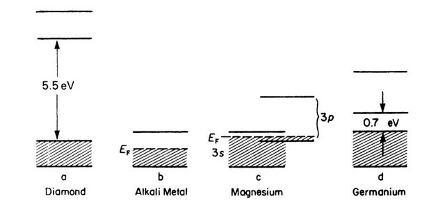
We mentioned in Section 6.4 that, because of the Pauli principle, each s-band of a crystal, consisting of N atoms, has space for 2N electrons, i.e., for two electrons per atom. If the highest filled s-band of a crystal is occupied by two electrons per atom, i.e., if the band is completely filled, we would expect that the electrons cannot drift through the crystal when an external electric field is applied (as it is similarly impossible to move a car in a completely occupied parking lot). An electron has to absorb energy in order to move. Keep in mind that for a completely occupied band higher energy states are not allowed. (We exclude the possibility of electron jumps into higher bands.) Solids in which the highest filled band is completely occupied by electrons are, therefore, insulators (Fig. 6.7(a)).
In solids with one valence electron per atom (e.g., alkali metals) the valence band is essentially half-filled. An electron drift upon application of an external field is possible; the crystal shows metallic behavior (Fig. 6.7(b)).
Bivalent metals should be insulators according to this consideration, which is not the case. The reason for this lies in the fact that the upper bands partially overlap, which occurs due to the weak binding forces of the valence electrons on their atomic nuclei (see Fig. 5.9).
Figure 6.7. Simplified representation for energy bands for (a) insulators, (b) alkali metals, (c) bivalent metals, and (d) intrinsic semiconductors.
If such an overlapping of bands occurs, the valence electrons flow in the lower portion of the next higher band, because the electrons tend to assume the lowest potential energy (Fig. 6.7(c)). As a result, bivalent solids may also possess partially filled bands. Thus, they are also conductors.
We shall see in topic 8 that the valence as well as the conduction bands of semiconductors can accommodate 4N electrons. Because germanium and silicon possess four valence electrons, the valence band is completely filled with electrons. Intrinsic semiconductors have a relatively narrow forbidden energy zone (Fig. 6.7(d)). A sufficiently large energy can, therefore, excite electrons from the completely filled valence band into the empty conduction band and thus provide some electron conduction.
This preliminary and very qualitative discussion on electronic conduction will be expanded substantially and the understanding will be deepened in Part II of this topic.
Effective Mass
We implied in the previous sections that the mass of an electron in a solid is the same as the mass of a free electron. Experimentally determined physical properties of solids, such as optical, thermal, or electrical properties, indicate, however, that for some solids the mass is larger while for others it is slightly smaller than the free electron mass. This experimentally determined electron mass is usually called the effective mass, m*. The deviation of m* from the free electron mass17 m0 can be easily appreciated by stating the ratio m*/m0, which has values slightly above or below 1 (see topic 4). The cause for the deviation of the effective mass from the free electron mass is usually attributed to interactions between the drifting electrons and the atoms in a crystal. For example, an electron which is accelerated in an electric field might be slowed down slightly because of "collisions" with some atoms. The ratio m*/m0 is then larger than 1. On the other hand, the electron wave in another crystal might have just the right phase in order that the response to an external electric field is enhanced. In this case, m*/m0 is smaller than 1.
We shall now attempt to find an expression for the effective mass. For this, we shall compare the acceleration of an electron in an electric field calculated by classical as well as by quantum mechanical means. At first, we write an expression for the velocity of an electron in an energy band.
We introduced in topic 2 the group velocity, i.e., the velocity with which a wave packet moves. Let o be the angular frequency and Ikl = 2p/1 the wave number of the electron wave. Then, the group velocity is, according to (2.10),
From this we calculate the acceleration
The relation between the energy E and the wave number IkI is known from the preceding sections. We now want to determine the factor dk/dt. Forming the first derivative of (4.7) (p = \k) with respect to time yields
Combining (6.14) with (6.13) yields
where F is the force on the electron. The classical acceleration can be calculated from Newton’s law (1.1)
Comparing (6.15) with (6.16) yields the effective mass
We see from (6.17) that the effective mass is inversely proportional to the curvature of an electron band. Specifically, if the curvature of E = f (k) at a given point in k-space is large, then the effective mass is small (and vice versa). When inspecting band structures (Fig. 5.4 or Figs. 5.21-5.24) we notice some regions of high curvature. These regions might be found, particularly, near the center or near the boundary of a Brillouin zone. At these places, the effective mass is substantially reduced and may be as low as 1% of the free electron mass m0. At points in k-space for which more than one electron band is found (r-point in Fig. 5.23, for example) more than one effective mass needs to be defined.
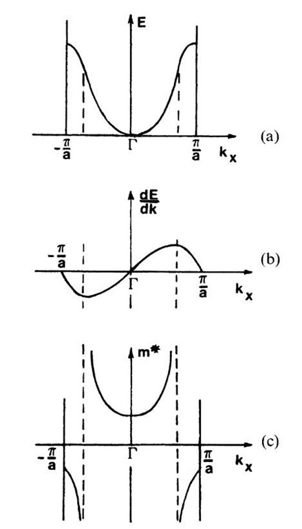
We shall demonstrate the k-dependence of the effective mass for a simple case and defer discussions about actual cases to Section 8.4. In Fig. 6.8(a) an ideal electron band within the first Brillouin zone is depicted.
Figure 6.8. (a) Simple band structure, as shown in Fig. 5.4. (b) First derivative and (c) inverse function of the second derivative of the curve shown in (a).
From this curve, both the first derivative and the reciprocal function of the second derivative, i.e., m*, have been calculated. These functions are shown in Fig. 6.8(b) and (c). We notice in Fig. 6.8(c) that the effective mass of the electrons is small and positive near the center of the Brillouin zone and eventually increases for larger values of kx. We likewise observe in Fig. 6.8(c) that electrons in the upper part of the given band have a negative effective mass. A negative mass means that the "particle" under consideration travels in the opposite direction to an applied electric force (and opposite to an electron.) An electron with a negative effective mass is called a "defect electron" or an "electron hole". (It is, however, common to ascribe to the hole a positive effective mass and a positive charge instead of a negative mass and a negative charge.) Electron holes play an important role in crystals whose valence bands are almost filled, e.g., in semiconductors. Solids which possess different properties in various directions (anisotropy) have a different m* in each direction. The effective mass is a tensor in this case. An electron/hole pair is called an "exciton".
It should be noted here for clarification that an electron hole is not identical with a positron. The latter is a subatomic particle like the electron, however with a positive charge. Positrons are emitted in the b-decay or are found in cosmic radiation. When positrons and electrons react with each other they are both annihilated under emission of energy.
Conclusion
The first part of this topic is intended to provide the reader with the necessary tools for a better understanding of the electronic properties of materials. We started our discussion by solving the Schrodinger equation for the free electron case, the bound electron case, and for electrons in a crystal. We learned that the distinct energy levels which are characteristic for isolated atoms widen into energy bands when the atoms are moved closer together and eventually form a solid. We also learned that the electron bands have "fine structure," i.e., they consist of individual "branches" in an energy versus momentum (actually k) diagram. We further learned that some of these energy bands are filled by electrons, and that the degree of this filling depends upon whether we consider a metal, a semiconductor, or an insulator. Finally, the degree to which electron energy levels are available within a band was found to be nonuniform. We discovered that the density of states is largest near the center of an electron band. All these relatively unfamiliar concepts will become more transparent to the reader when we apply them in the topics to come.


