Ionic Conduction
In ionic crystals (such as the alkali halides), the individual lattice atoms transfer electrons between each other to form positively charged cations and negatively charged anions. The binding forces between the ions are electrostatic in nature and are thus very strong. The room-temperature conductivity of ionic crystals is about twenty-two orders of magnitude smaller than the conductivity of typical metallic conductors (Fig. 7.1). This large difference in s can be understood by realizing that the wide band gap in insulators allows only extremely few electrons to become excited from the valence band into the conduction band.
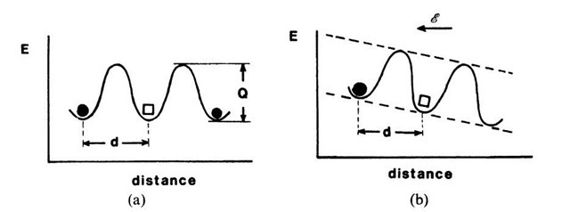
The main contribution to the electrical conduction in ionic crystals (as little as it may be) is, however, due to a mechanism that we have not yet discussed, namely, ionic conduction. Ionic conduction is caused by the movement of some negatively (or positively) charged ions which hop from lattice site to lattice site under the influence of an electric field, see Fig. 9.8 (b). (This type of conduction is similar to that which is known to occur in aqueous electrolytes.) This ionic conductivity
is, as outlined before (8.13), the product of three quantities. In the present case, Nion is the number of ions per unit volume that can change their position under the influence of an electric field and mion is the mobility of these ions.
Figure 9.8. Schematic representation of a potential barrier, which an ion (•) has to overcome to exchange its site with a vacancy (□). (a) Without an external electric field; (b) with an external electric field. d = distance between two adjacent, equivalent lattice sites; Q = activation energy.
In order for ions to move through a crystalline solid, they must have sufficient energy to pass over an energy barrier (Fig. 9.8). Further, an equivalent lattice site next to a given ion must be empty in order for an ion to be able to change its position. Thus, Nion in (9.1) depends on the vacancy concentration in the crystal (i.e., on the number of Schottky defects11). In short, the theory of ionic conduction contains essential elements of diffusion theory, with which the reader might be familiar.
Diffusion theory links the mobility of the ions, which is contained in (9.1), with the diffusion coefficient, D, through the Einstein relation,
(Note that (9.2) implies that one charge unit per atom is transported.)
The diffusion coefficient varies with temperature; this dependence is commonly expressed by an Arrhenius equation,
where Q is the activation energy for the process under consideration (Fig. 9.8), and D0 is a pre-exponential factor that depends on the vibrational frequency of the atoms and some structural parameters. Combining (9.1) through (9.3) yields
Equation (9.4) is shortened by combining the pre-exponential constants into a0:
Taking the natural logarithm yields
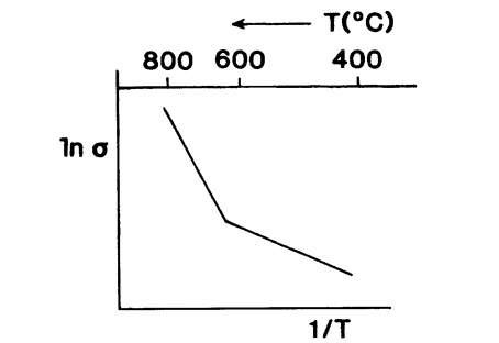
Equation (9.6) suggests that if ln aion is plotted versus 1/T, a straight line with a negative slope would result. Figure 9.9 depicts schematically a plot of ln a versus 1/T as experimentally found for alkali halides. The linear ln a versus 1/T relationship indicates that Fig. 9.9 is an actual representation of (9.6).
Figure 9.9. Schematic representation of In a versus 1/T for Na+ ions in sodium chloride.
The slopes of the straight lines in Arrhenius plots are utilized to calculate the activation energy of the processes under consideration. We notice in Fig. 9.9 two temperature regions representing two different activation energies: at low temperatures, the activation energy is small, the thermal energy is just sufficient to allow the hopping of ions into already existing vacancy sites. This temperature range is commonly called the extrinsic region. On the other hand, at high temperatures, the thermal energy is large enough to create additional vacancies. The related activation energy is thus the sum of the activation energies for vacancy creation and ion movement. This temperature range is called the intrinsic region.
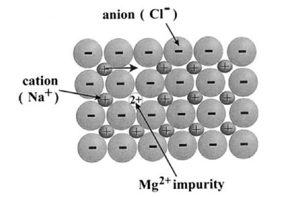
So far, we have not been very specific in describing the circumstances of vacancy formation in an ionic crystal. Now, we have to realize that whenever vacant lattice sites are created, an overall charge neutrality needs to be maintained. The latter is the case when both a cation and an anion are removed from a lattice. Another permissible mechanism is the formation of a vacancy-interstitial pair (Frenkel defect). More often, however, vacancies are created as a consequence of introducing differently charged impurity atoms into an ionic lattice, i.e., by replacing, say, a monovalent metal atom with a divalent atom. In order to maintain charge neutrality in this case, a positively charged vacancy needs to be introduced. For example, if a divalent Mg2+ ion substitutes for a monovalent Na+ ion, one extra Na+ ion has to be removed to restore charge neutrality, see Fig. 9.10. Or, if zirconia (ZrO2) is treated with CaO (to produce the technically important calcia-stabilized zirconia), the Ca2+ ions substitute for Zr4+ ions and an anion vacancy needs to be created to maintain charge neutrality. Nonstoichio-metric compounds contain a high amount of vacancies even at relatively low temperatures, whereas in stoichiometric compounds vacancies need to be formed by elevating the temperature.
In principle, both cations and anions are capable of moving simultaneously under the influence of an electric field. It turns out, however, that in most alkali halides the majority carriers are provided by the (smaller) metal ions, whereas in other materials, such as the lead halides, the conduction is predominantly performed by the halide ions.
Figure 9.10. Schematic representation of a {100} plane of an ionic crystal having the NaCl structure. The diffusion of a cation into a cation vacancy is shown. Also depicted is the creation of a cation vacancy when replacing a Na+ ion with a Mg2+ ion.
So far, it was implied that the materials under consideration are single crystals. For polycrystalline materials, however, it appears reasonable to assume that the vacant lattice sites provided by the grain boundaries would be utilized by the ions as preferred paths for migration, thus enhancing the conductivity. This has indeed been experimentally observed for alkali ions.
One piercing question remains to be answered: If ionic conduction entails the transport of ions, i.e., of matter from one electrode to the other, would this not imply some segregation of the constituents? Indeed, a pile-up of mobile ions at the electrodes has been observed for long-lasting experiments with a concomitant induced electric field in the opposite direction to the externally applied field. As a consequence the conductivity decreases gradually over time. Of course, this does not happen when nonblocking electrodes are utilized which provide a source and a sink for the mobile species.
Conduction in Metal Oxides
Metal oxides do not actually represent a separate class of conducting materials on their own. Indeed, they can be insulating, such as TiO2, have metallic conduction properties, such as TiO, or be semiconducting. For understanding the mechanisms involved in metal oxides, e.g., in the aforementioned titanium oxides, it is helpful to inspect the table in topic 3. Oxygen is seen there to have four 2p-electrons in its outermost shell. Two more electrons will bring O2" into the closed-shell configuration and four electrons are obviously needed to accomplish the same for two oxygen ions, such as in TiO2. These four electrons are provided by the titanium from its 3d- and 4s-shells. Thus, in the case of TiO2, all involved elements are in the noble gas configuration. Since ionic bonds are involved, any attempted removal of electrons would require a considerable amount of thermal energy. TiO2 is, consequently, an insulator having a wide band gap. Not so for TiO. Since only two titanium valence electrons are needed to fill the 2p-shell of one oxygen ion, two more titanium electrons are free to serve as conduction electrons. Thus, TiO has metallic properties with a s in the 103 O"1 cm"1 range.
A refinement of our understanding is obtained by considering the pertinent electron bands. TiO has, according to the aforementioned explanations, a filled oxygen 2p-valence band and an essentially empty titanium 4s-conduction band. Also involved is a narrow titanium 3d-band which is partially filled by the above-mentioned two electrons. The conduction in TiO takes place, therefore, in the titanium 3d-band, which can host, as we know, a total of 10 electrons.
We discuss zinc oxide as a next example. Zn in ZnO has two valence 4s-electrons which transfer to the oxygen 2p-band. ZnO, if strictly stoichio-metric, has, thus, a filled valence 2p-band and an empty zinc 4s-band employing a gap energy of 3.3 eV. Stoichiometric ZnO is therefore an insulator or a wide-band-gap semiconductor. Now, if interstitial zinc atoms (or oxygen vacancies) are introduced into the lattice (by heating ZnO in a reducing atmosphere, which causes neutral oxygen to leave the crystal) then the valence electrons of these zinc interstitials are only loosely bound to their nuclei. One of these two electrons can easily be ionized (0.05 eV) and acts therefore as a donor. Nonstoichiometric ZnO is, consequently, an n-type semiconductor. The same is incidentally true for nonstoi-chiometric Cu2O (see topic 3), an established semiconducting material from which Cu/Cu2O Schottky-type rectifiers were manufactured long before silicon technology was invented.
Another interesting metal oxide is SnO2 (sometimes doped with In2O3), which is transparent in the visible region and which is a reasonable conductor in the 1 O"1 cm"1 range. It is used in optoelectronics to provide electrical contacts without blocking the light from reaching a device. It is known as indium-tin-oxide or ITO.
Finally, we discuss NiO. Again, a filled oxygen 2p-band and an empty nickel 4s-band are involved. In order to form the nickel 3d-bands required for conduction, a substantial overlap of the 3d-wave functions would be required by quantum mechanics. Band structure calculations show, however, that these interactions do not take place. Instead, deep-lying localized electron states in the forbidden band close to the upper edge of the valence band are observed. Thus, no 3d-band conduction can take place, which results in stoichiometric NiO being an insulator. Nonstoichiometry (obtained by removing some nickel atoms, thus creating cation vacancies) causes NiO to become a p-type semiconductor.
Amorphous Materials (Metallic Glasses)
Before we discuss electrical conduction in amorphous materials, we need to clarify what the term amorphous means in the present context. Strictly speaking, amorphous implies the random arrangement of atoms, the absence of any periodic symmetry, or the absence of any crystalline structure. One could compare the random distribution of atoms with the situation in a gas, as seen in an instantaneous picture. Now, such a completely random arrangement of atoms is seldom found even in liquids, much less in solids. In actuality, the relative positions of nearest neighbors surrounding a given atom in an amorphous solid are almost identical to the positions in crystalline solids because of the ever-present binding forces between the atoms. In short, the atomic order in amorphous materials is restricted to the nearest neighbors. Amorphous materials exhibit, therefore, only short-range order. In contrast to this, the exact positions of the atoms that are farther apart from a given central atom cannot be predicted. This is particularly the case when various kinds of stacking orders, i.e., if polymorphic modifications, are possible. As a consequence one observes atomic disorder at long range. The term amorphous solid should therefore be used cum grano salis. We empirically define materials to be amorphous when their diffraction patterns consist of diffuse rings, rather than sharply defined Bragg rings, as are characteristic for polycrystalline solids.
So far we have discussed positional disorder only as it might be found in pure materials. If more than one component is present in a material, a second type of disorder is possible: The individual species might be randomly distributed over the lattice sites; i.e., the species may not be alternately positioned as is the case for, say, sodium and chlorine atoms in NaCl. This random distribution of species is called compositional disorder.
The best-known representative of an amorphous solid is window glass, whose major components are silicon and oxygen. Glass is usually described as a supercooled liquid.
Interestingly enough, many elements and compounds that are generally known to be crystalline under equilibrium conditions can also be obtained in the nonequilibrium amorphous state by applying rapid solidification techniques, i.e., by utilizing cooling rates of about 105 K/s. These cooling rates can be achieved by fast quenching, melt spinning, vapor deposition, sputtering, radiation damage, filamentary casting in continuous operation, spark-processing, etc. The degree of amorphousness (or, the degree of short range order) may be varied by the severity of the quench. The resulting metallic glasses, or glassy metals, have unusual electrical, mechanical, optical, magnetic, and corrosion properties and are therefore of considerable interest. Amorphous semiconductors (consisting, e.g., of Ge, Si, GeTe, etc.) have also received substantial attention because they are relatively inexpensive to manufacture, have unusual switching properties, and have found applications in inexpensive photovoltaic cells.
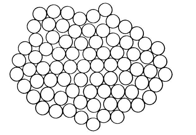
We now turn to the atomic structure of amorphous metals and alloys. They have essentially nondirectional bonds. Thus, the short-range order does not extend beyond the nearest neighbors. The atoms must be packed together tightly, however, in order to achieve the observed density. There are only a limited number of ways of close packing. One way of arranging the atoms in amorphous metals is depicted by the dense random packing of hard spheres model (Fig. 9.11). This Bernal model is considered as the ideal amorphous state. No significant regions of crystalline order are present. In transition metal-metalloid compounds (such as Ni-P) it is thought that the small metalloid atoms occupy the holes which occur as a consequence of this packing (Bernal-Polk model).
The atoms in amorphous semiconductors, on the other hand, do not arrange themselves in a close-packed manner. Atoms of group IV elements are, as we know, covalently bound. They are often arranged in a continuous random network with correlations in ordering up to the third or fourth nearest neighbors (Fig. 9.12(b) and (c)). Amorphous pure silicon contains numerous dangling bonds similar to those found in crystalline silicon in the presence of vacancies (Fig. 9.12(a)).
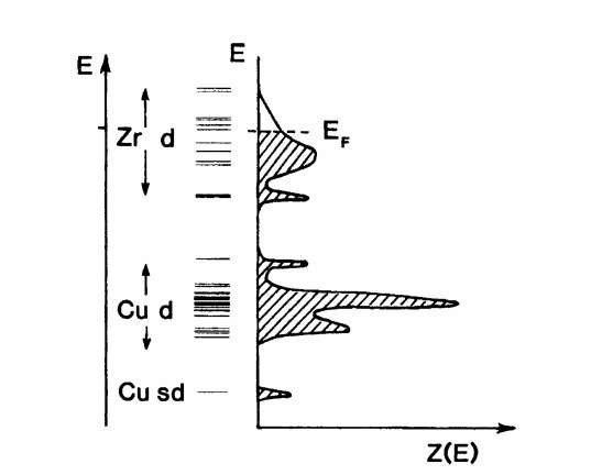
Since amorphous solids have no long-range crystal symmetry, we can no longer apply the Bloch theorem, which led us in Section 4.4 from the distinct energy levels for isolated atoms to the broad quasi-continuous bands for crystalline solids. Thus, the calculation of electronic structures for amorphous metals and alloys has to use alternate techniques, e.g., the cluster model approach. This method has been utilized to calculate the electronic structure of amorphous Zr-Cu (which is a representative of a noble metal-transition metal metallic glass). A series of clusters were assumed which exhibit the symmetry of the close-packed lattices fcc (as for Cu) and hcp18 (as for Zr).
Figure 9.11. Two-dimensional schematic representation of a dense random packing of hard spheres (Bernal model).
Figure 9.12. Defects in crystalline and amorphous silicon. (a) Monovacancy in a crystalline semiconductor; (b) one and (c) two dangling bonds in a continuous random network of an amorphous semiconductor. (Note the deviations in the interatomic distances and bond angles).
Figure 9.13. Schematic representation of the molecular orbital energy level diagram and the density of states curves for Zr-Cu clusters. The calculated density of states curves agree reasonably well with photoemission experiments.
The energy level diagram depicted in Fig. 9.13 shows two distinct "bands" of levels. The lower band consists primarily of copper d-levels, while the upper band consists mainly of zirconium d-levels. A sort of gap separates the two bands of levels. Even though the concept of quasi-continuous energy bands is no longer meaningful for amorphous solids, the density of states concept still is, as can be seen in Fig. 9.13. We notice that the Fermi energy is located in the upper part of the zirconium levels. Further, we observe partially filled electron states. This has two interesting consequences. First, we expect metal-like conduction. Second, Z(E) near EF is small, which suggests relatively small values for the conductivity (see (7.26)). Indeed, s for Cu-Zr is comparable to that of poor metallic conductors (i.e., approximately 5 x 10³ 1/O cm).
The electrical resistivity of many metallic glasses (such as Pd80Si20 or Fe32Ni36Cr14P12B619) stays constant over a fairly wide temperature range, up to the temperature which marks the irreversible transition from the amorphous into the crystalline state. This makes these alloys attractive as resistance standards. The mean free path for electrons in metallic glasses is estimated to be about 1 nm.
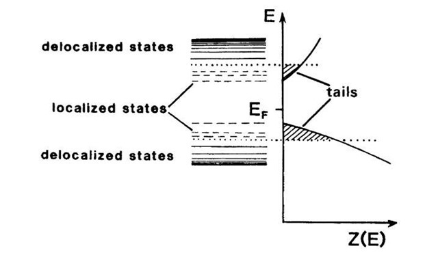
The energy level diagrams and the density of states curves for amorphous semiconductors are somewhat different from those for amorphous metals. Because of the stronger binding forces which exist between the atoms in covalently bound materials, the valence electrons are tightly bound, or localized. As a consequence, the density of states for the localized states extends into the "band gap" (Fig. 9.14). This may be compared to the localized impurity states in doped crystalline semiconductors, which are also located in the band gap. Thus, we observe density of states tails. These tails may extend, for some materials, so far into the gap that they partially overlap. In general, however, the density of electron and hole states for the localized levels is very small.
The electrical conductivity for amorphous semiconductors, sA, depends, as usual (8.13), on the density of carriers, NA, and the mobility of these carriers, mA:
The density of carriers in amorphous semiconductors is extremely small, because all electrons are, as said before, strongly bound (localized) to their respective nuclei.
Figure 9.14. Localized and delocalized states and density of states Z(E) for amorphous semiconductors. Note the band tails, which are caused by the localized states.
Likewise, the mobility of the carriers is small because the absence of a periodic lattice causes substantial incoherent scattering. As a consequence, the room-temperature conductivity in amorphous semiconductors is generally very low (about 10-7 1/O cm).
Some of the localized electrons might occasionally acquire sufficient thermal energy to overcome barriers which are caused by potential wells of variable depth and hop to a neighboring site. Thus, the conduction process in amorphous semiconductors involves a (temperature-dependent) activation energy, QA, which leads to an equation similar to (9.5), describing a so-called variable-range hopping
Equation (9.8) states that the conductivity in amorphous semiconductors increases exponentially with increasing temperature, because any increase in thermal energy provides additional free carriers.
The application of amorphous silicon for photovoltaic devices (see Section 8.7.6) will be discussed briefly in closing because of its commercial, as well as scientific, significance. If silicon is deposited out of the gas phase on relatively cold (<500°C) substrates (utilizing silane or sputtering), a structure as shown in Fig. 9.12 (b) and (c) results. Doping is virtually not possible in this condition since any free charge carriers recombine immediately with the dangling bonds. However, hydrogen, if added during deposition and incorporated into the solid, neutralizes the unsaturated valencies (and reduces internal strain in the lattice network). This results in hydrogenated amorphous silicon, which is, in its properties, quite comparable to crystalline silicon. Doping can be accomplished during deposition. This way, semiconducting materials can be produced which vary in their conductivity between 10-11 and 10-2 O-1 cm depending on doping (see Fig. 7.1). Commercial flat-plate solar cells of this type have an efficiency of about 8% compared to 14% efficiency for commercial single-crystal silicon technology. The price (and the consumption of power during manufacturing) is, however, only one-half of that for crystalline silicon, mainly because of the simpler way of deposition (see Section 8.7.6).
The understanding of amorphous metals, alloys, and semiconductors is still in its infancy. Future developments in this field should be followed with a great deal of anticipation because of the potentially significant applications which might arise in the years to come.
Xerography
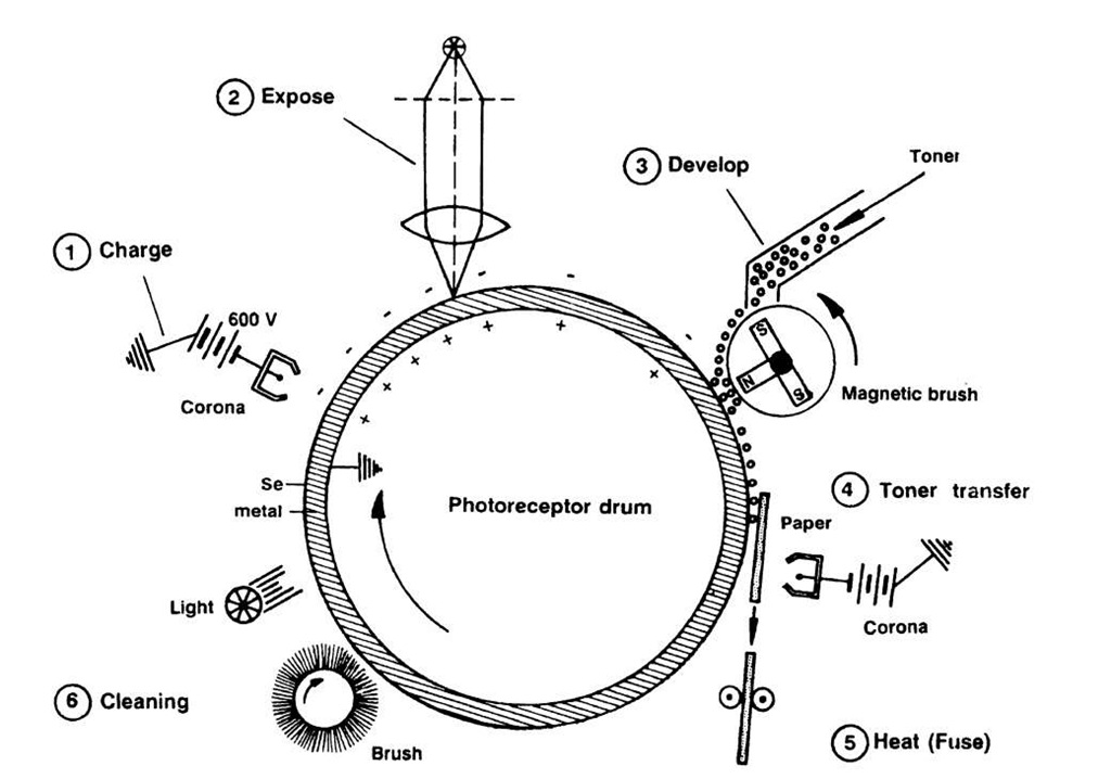
Xerography (from the Greek "dry writing") or electrophotography is an important application of amorphous semiconductors such as amorphous selenium or amorphous silicon, etc. (They have been recently replaced, however, by polyvinylcarbazole.) Such a material, when deposited on a cylindrically shaped metallic substrate, constitutes the photoreceptor drum, as shown in Fig. 9.15.
Before copying, the photoreceptor is electrostatically charged by means of a corona wire to which a high voltage is applied (Step 1). Amorphous semiconductors are essentially insulators (see above) which hold this electric charge reasonably well, as long as they are kept in the dark. If, however, light which has been reflected from the document to be copied falls on the photoreceptor, electron-hole pairs are formed, causing the photoreceptor to become conducting. This process discharges the affected parts on the drum, creating a latent image on the photoreceptor, i.e., a pattern consisting of charged and neutral areas. At the next step, electrostatically charged and pigmented polymer particles (called toner) are brought into contact with the drum. The toner clings to the charged areas only. Commonly, a two-component toner is utilized; one part consists of magnetically soft particles. They form brush-type chains under the influence of a magnetic field which is caused by permanent magnets that are rotated inside a cylinder (see Fig. 9.15, Step 3). Eventually, the toner on the photoreceptor is electrostatically transferred to a piece of paper by properly corona-charging the back of the paper.
Figure 9.15. Schematic representation of the electrophotography process. The individual steps are explained in the text.
Finally, the toner is fused to the paper by heat. A cleaning and photodischarging process prepares the photoreceptor drum for the next cycle.
Laser printers use the same principle. To create the latent image, the laser light is periodically scanned across the rotating photoreceptive drum by means of a rotating multisurface mirror. The spectral sensitivity of the amorphous semiconductor has to be matched to the wavelength of the laser light. Amorphous silicon (maximal photosensitivity near 700 nm) in conjunction with a helium-neon laser (see Table 13.1) is a usable combination.
![tmp8-11_thumb[2] tmp8-11_thumb[2]](http://what-when-how.com/wp-content/uploads/2011/07/tmp811_thumb2_thumb.jpg)
![tmp8-12_thumb[2] tmp8-12_thumb[2]](http://what-when-how.com/wp-content/uploads/2011/07/tmp812_thumb2_thumb.jpg)
![tmp8-13_thumb[2] tmp8-13_thumb[2]](http://what-when-how.com/wp-content/uploads/2011/07/tmp813_thumb2_thumb.jpg)
![tmp8-14_thumb[2] tmp8-14_thumb[2]](http://what-when-how.com/wp-content/uploads/2011/07/tmp814_thumb2_thumb.jpg)
![tmp8-15_thumb[2] tmp8-15_thumb[2]](http://what-when-how.com/wp-content/uploads/2011/07/tmp815_thumb2_thumb.jpg)

![tmp8-21_thumb[2] tmp8-21_thumb[2]](http://what-when-how.com/wp-content/uploads/2011/07/tmp821_thumb2_thumb.jpg)
![tmp8-23_thumb[2] tmp8-23_thumb[2]](http://what-when-how.com/wp-content/uploads/2011/07/tmp823_thumb2_thumb.jpg)
