Conducting Polymers and Organic Metals
Materials which are electrical (and thermal) insulators are of great technical importance and are, therefore, used in large quantities in the electronics industry, e.g., as handles for a variety of tools, as coatings for wires, or as casings for electrical equipment. Most polymeric materials have the required insulating properties and have been used for decades for this purpose. It came, therefore, as a surprise when it was discovered in the late 1970′s that some polymers and organic substances may have electrical properties which resemble those of conventional semiconductors, metals, or even superconductors. We shall focus our attention mainly on these materials. This does not imply that the predominance of applications of polymers is in the conductor field. Quite the contrary is true. Nevertheless, conducting polymers (also called synthetic metals) steadily gain ground compared to insulating polymers.
Initially, conducting polymers were unstable in air or above room temperature. In addition, some dopants, used to impart a greater conductivity, were toxic, and the doping made the material brittle. However, more recently, stable conducting polymers were synthesized which have as an added benefit an optical transparency across the entire visible spectrum. Among them, poly(3,4-ethylenedioxythiophene) (PEDOT) and its derivatives enjoy now multi-ton productions, in particular for antistatic layers in photographic films. These conducting layers are beneficial for the prevention of friction-induced static electricity, which causes, on discharge, flashes of light, thus, pre-exposing the light-sensitive emulsion. Other uses of PEDOT are transparent electrodes for inorganic electroluminescent devices, anti-static treatments of plastics and cathode ray tubes, electrodes for capacitors, sensors, rechargeable batteries, photovoltaic devices, and packaging of electronic components. PEDOT films can be heated in air at 100° C for over 1000 hours with hardly any change in conductivity.
We now attempt to discuss conducting polymers in the light of solid-state physics. Conventional solid-state physics deals preferably with the properties of well-defined regular arrays of atoms. We have learned in topic 7 that a periodic array of lattice atoms is imperative for coherent scattering of electron waves and thus for a high conductivity. Further, the periodic arrangement of atoms in a crystal and the strong interactions between these atoms causes, as explained in Section 4.4, a widening of energy levels into energy bands.
We know that highly conducting materials such as metals are characterized by partially filled bands, which allow a free motion of the conduction electrons in an electric field. Insulators and semiconductors, on the other hand, possess (at least at 0 K) completely filled valence bands and empty conduction bands. The difference in band structure between crystalline insulators and semiconductors is a matter of degree rather than of kind: insulators have wide gaps between valence and conduction bands whereas the energy gaps for semiconductors are narrow. Thus, in the case of semiconductors, the thermal energy is large enough to excite some electrons across the gap into the conduction band. The conductivity in pure semiconductors is known to increase (exponentially) with increasing temperature and decreasing gap energy (8.14), whereas the conductivity in metals decreases with increasing temperature (Fig. 7.7). Interestingly enough, most conducting polymers have a temperature dependence of the conductivity similar to that of semiconductors. This suggests that certain aspects of semiconductor theory may be applied to conducting polymers. The situation regarding polymers cannot be described, however, without certain modifications to the band model brought forward in the previous topics. This is due to the fact that polymeric materials may exist in amorphous as well as in crystalline form or, more commonly, as a mixture of both. This needs to be discussed in some detail.
Polymers consist of molecules which are long and chainlike. The atoms that partake in such a chain (or macromolecule) are regularly arranged along the chain. Several atoms combine and form a specific building block, called a monomer, and thousands of monomers combine to a polymer. As an example, we depict polyethylene, which consists of repeat units of one carbon atom and two hydrogen atoms, Fig. 9.1(a). If one out of four hydrogen atoms in polyethylene is replaced by a chlorine atom, polyvinylchloride (PVC) is formed upon polymerization (Fig. 9.1(b)). In polystyrene, one hydrogen atom is replaced by a benzene ring. More complicated macromolecules may contain side chains attached to the main link. They are appropriately named "branched polymers". Macromolecules whose backbones consist largely of carbon atoms, as in Fig. 9.1, are called "organic" polymers.
Figure 9.1. (a) Polyethylene. (b) Polyvinylchloride. (The dashed enclosures mark the repeat unit. Polyethylene is frequently depicted as two CH2 repeat units for historical reasons).
The binding forces that hold the individual atoms in polymers together are usually covalent and sometimes ionic in nature. Covalent forces are much stronger than the binding forces in metals. They are based on the same interactions that are responsible for forming a hydrogen molecule from two hydrogen atoms. Quantum mechanics explains covalent bonds by showing that a lower energy state is achieved when two equal atomic systems are closely coupled and in this way exchange their energy (see Section 16.2). In organic polymers each carbon atom is often bound to four atoms (see Fig. 9.1) because carbon has four valencies.
In contrast to the strong binding forces between the atoms within a polymeric chain, the secondary interactions between the individual macro-molecules are usually weak. The latter are of the Van der Waals type, i.e., they are based on forces which induce dipole moments in the molecules. (Similar weak interactions exist for noble gases such as argon, neon, etc.)
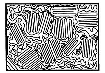
In order to better understand the electronic properties of polymers by means of the electron theory and the band structure concept, one needs to know the degree of order or the degree of periodicity of the atoms, because only ordered and strongly interacting atoms or molecules lead, as we know, to distinct and wide electron bands. Now, it has been observed that the degree of order in polymers depends on the length of the molecules and on the regularity of the molecular structure. Certain heat treatments may influence some structural parameters. For example, if a simple polymer is slowly cooled below its melting point, one might observe that some macro-molecules align parallel to each other. The individual chains are separated by regions of supercooled liquid, i.e., of amorphous material (Fig. 9.2). Actually, slow cooling yields, for certain polymers, a highly crystalline structure.
In other polymers, the cooling procedure might cause the entire material to go into a supercooled-liquid state. In this state the molecules can be considered to be randomly arranged. After further cooling, below a glass transition temperature, the polymer might transform itself into a glassy amorphous solid which is strong, brittle, and insulating. However, as stated before, we shall concern ourselves mainly with polymers that have a high degree of crystallinity. Amorphous materials will be discussed in Section 9.4.
Figure 9.2. Simplified representation of a semicrystalline polymer (folded-chain model).
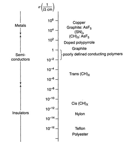
A high degree of crystallinity and a relatively high conductivity have been found in polyacetylene, which is the simplest conjugated organic polymer. It is considered to be the prototype of a conducting polymer. A conjugated polymer has alternating single and double bonds between the carbons (see Fig. 9.3, which should be compared to Fig. 9.1(a)). Two principle isomers are important: in the trans form, the hydrogen atoms are alternately bound to opposite sides of the carbons (Fig. 9.3(b)), whereas in the cis form the hydrogen atoms are situated on the same side of the double-bond carbons (Fig. 9.3(a)). Trans-polyacetylene is obtained as a silvery, flexible film that has a conductivity comparable to that of silicon (Fig. 9.4).
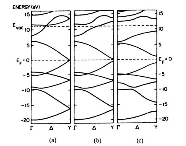
Figure 9.5 shows three band structures for trans-(CH)x assuming different distances between the carbon atoms. In Fig. 9.5(a) all carbon bond lengths are taken to be equal. The resulting band structure is found to be characteristic for a metal, i.e., one obtains distinct bands, the highest of which is partially filled by electrons. Where are the free electrons in the conduction band coming from? We realize that the electrons in the double bond of a conjugated polymer (called the p-electrons) can be considered to be only loosely bound to the neighboring carbon atoms. Thus, one of these electrons is easily disassociated from its carbon atom by a relatively small energy, which may be provided by thermal energy. The delocalized electrons may be accelerated as usual in an electric field.
Figure 9.3. Theoretical isomers of polyacetylene (a) cis-transoidal isomer, (b) trans-transoidal isomer. Polyacetylene is synthesized as cis-(CH)x and is then isomerized into the trans-configuration by heating it at 150°C for a few minutes.
Figure 9.4. Conductivities of polymers in ![]()
In reality, however, a uniform bond length between the carbon atoms does not exist in polyacetylene. Instead, the distances between the carbon atoms alternate because of the alternating single and double bonds. Band structure calculations for this case show, interestingly enough, some gaps between the individual energy bands. The resulting band structure is typical for a semiconductor (or an insulator)! The width of the band gap near the Fermi level depends mainly on the extent of alternating bond lengths (Fig. 9.5(b) and (c)).
It has been shown that the band structure in Fig. 9.5(b) best represents the experimental observations. Specifically, one finds a band gap of about 1.5 eV and a total width of the conduction band of 10-14 eV. The effective mass m* is 0.6m0 at k = 0 and 0.1m0 at k = p/a. Assuming t ! 10"14 s, the free carrier mobility, m, along a chain is calculated to be about 200 cm2/V s. The latter quantity is, however, hard to measure since the actual drift mobility in the entire solid is reduced by the trapping of the carriers which occurs during the "hopping" of the electrons between the individual macro-molecules. In order to improve the conductivity of (CH)x one would attempt to decrease the disparity in the carbon-carbon bond lengths, thus eventually approaching the uniform bond length as shown in Fig. 9.5(a).
Figure 9.5. Calculated band structure of trans-(CH)x for different carbon-carbon bond lengths: (a) uniform (1.39 A); (b) weakly alternating (C=C, 1.36 A; C—C, 1.43 A); and (c) strongly alternating (C=C, 1.34 A; C—C, 1.54 A). Note the band gaps at Y as bond alternation occurs.
*It should be noted in passing that chemists, particularly when dealing with organic molecules, utilize a different terminology for presenting the same information that has been just described. This will be briefly explained here for completeness. This alternative representation involves so-called HOMO and LUMO levels which are acronyms for highest occupied molecular orbitals and lowest unoccupied molecular orbitals, respectively. An orbital is described as a region in space about the nucleus in which there is a 95% probability of finding an electron, see topic 3. (Each of those orbitals can be occupied with maximal two electrons having opposite spin.) In short, the HOMO level is essentially analogous to (or better, a part of) the valence band, which we have used in previous ts and in Fig. 9.5(b) and (c). Likewise, the LUMO level is part of the conduction band. The energy difference between the HOMO and LUMO levels is considered to be the band gap. Now, if there is an aggregate of molecules, the interaction between these individual molecules leads to a splitting of the HOMO and LUMO levels having slightly different energies. These sublevels have different vibrational energies. Once a large number of molecules are in close proximity, these energy levels overlap to form a continuum, that is, essentially an energy band.
A further piece of nomenclature may be added. In topic 3, we explain the meaning of s and p orbitals. These binding orbitals are in their ground state and are therefore occupied by electrons. Once electrons are instead in an excited state they are termed to be in s* and p* orbitals, respectively.The p orbital is often set identical with the HOMO level and the p* orbital is equivalent to the LUMO level. As already mentioned above, the energy difference between the HOMO and LUMO levels, that is, the separation between p and p* orbitals is the band gap energy, Eg, which is typically between 1 and 4 eV for organic semiconductors.
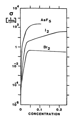
Polyacetylene, as discussed so far, should be compared to conventional intrinsic semiconductors. Now, we know from Section 8.3 that the conductivity of semiconductors can be substantially increased by doping. The same is true for polymer-based semiconductors. Indeed, arsenic-pentafluoride-doped trans-polyacetylene has a conductivity which is about seven orders of magnitude larger than undoped trans-(CH)x. Thus, s approaches the conductivity of metals, as can be seen in Figs. 9.4 and 9.6. Many oxidants cause p-type semiconductors, whereas alkali metals are n-type dopants.
Figure 9.6. Conductivity change of polyacetylene as a result of doping.
The doping is achieved through the vapor phase or by electrochemical methods. The dopant molecules diffuse between the (CH)x chains and provide a charge transfer between the polymer and the dopant. The additional element ends up as an anion when it is an acceptor and as a cation when it is a donor. Among other (albeit nontoxic) dopants is n-dodecyl sulfonate (soap). A word of caution, when using the word "doping", should be added at this point. In semiconductor physics, doping means extremely small additions of impurity elements. In polymers, much larger quantities of additional substances are used, ranging from one tenth of a percent up to 20-40%.
A refinement in the description of the conduction mechanism in polyacetylene can be provided by introducing the concept of solitons. A soliton is a structural distortion in a conjugated polymer and is generated when a single bond meets another single bond, as shown in Fig. 9.7. At the distortion point a localized nonbonding electron state is generated, similar to an n-type impurity state in a silicon semiconductor. In other words, a negative charge is associated with a soliton, as seen in Fig. 9.7 (involving two carbon bonds and one hydrogen bond to a carbon ion). The result is a localized level in the center of the forbidden band. It is believed that when an electron is excited from the valence band into the conduction band (leaving a hole in the valence band) this electron-hole pair decays in about 10"12 s into a more stable soliton-antisoliton pair.
Near the center of a soliton, the bond lengths are equal. We recall that uniform bond lengths constitute a metal. Thus, when many solitons have been formed and their spheres of influence overlap, a metal-like conductor would result.
It is also conceivable that one of the double bonds next to a soliton switches over to a single bond. If this switching occurs consecutively in one direction, a soliton wave results. This can be compared to a moving electron.
Up to now, we discussed mainly the properties of polyacetylene. Over the last 30 years additional conductive polymers have been discovered. They include polyanilines, polypyrroles, polythiophenes, polyphenylenes, poly(p-phenylene vinylene) and their derivatives. Of these, the polyaniline family can be easily processed at low cost but might yield toxic (carcinogenic) products upon degradation. Others are more "environmentally friendly" but are insoluble. On the other hand, the above-mentioned PEDOT (developed by Bayer AG in Germany) can be made water-soluble by utilizing poly (styrenesulfonate) (PSS) as a dopant during polymerization.
Figure 9.7. A broken symmetry in polyacetylene creates a soliton.
Its antistatic and other properties have been mentioned already above. With respect to carbon-free polymers, the chains in inorganic poly(sulfur nitride) consist of alternating sulfur and nitrogen atoms. Because of the different valencies of the S2- and N3- ions, (SN)x is an electron-deficient material with an alternating bond structure. The bond length alternation is not severe, so that (SN)x has a room-temperature conductivity of about 103 ohm1 cm-1 along the chain direction. The conductivity increases with a reduction in temperature. At temperatures close to 0 K, poly(sulfur nitride) becomes superconducting. In brominated (SN)x the Br- and Br- ions are aligned along the chain axis, giving rise to a one-dimensional superlattice.
In graphite, "molecules" consists of "sheets" of carbon atoms. The conductivity is found to be nearly metallic, at least parallel to the layers (Fig. 9.4). AsF5-doped graphite has an even higher conductivity. The conduction is increased by producing a mixture of easily ionized electron donors and electron acceptors. The charge is then shared between the donors and acceptors. These materials are called charge-transfer complexes.
An isolated atomic plane of graphite, that is, a monolayer of carbon atoms, is called graphene. It can be identified in the high-resolution electron microscope as a two-dimensional (2D) honeycomb lattice (six-member carbon ring), where the distance between next-neighbor atoms is 0.14 nm. Graphene has extraordinary physical properties and is therefore intensely studied both, from a theoretical point of view as well as experimentally because of its potential applications in computer technology and other fields. Specifically, intrinsic graphene is a semi-metal whereas extrinsic graphene is a semiconductor whose band gap can be tuned from 0 to 0.25 eV. It has a zero effective mass for electrons and holes at low energies, a high room temperature electron mobility (>1.5 m2/V s, compared to 0.15 m2/V s for Si, see topic 4) leading to a mean free path of several microns, a sheet conductivity of 106 1/(O cm) (which is larger than that for Ag, see Fig. 7.1), and a thermal conductivity around 5 x 10³ W/m K (which is higher than that for diamond, see Table 19.3). Moreover, graphene seems to be one of the strongest materials, having a breaking strength 200 times larger than steel. It absorbs about 2.3% of white light despite its monolayer thickness (which makes it visible in transmission). Finally, the quantum Hall effect has been observed in graphene at room temperature (see Section 8.5). No wonder that it is speculated that graphene would eventually replace silicon for ultra-large-scale integrated electronic devices. Indeed, n-and p-type semiconductors, a bipolar transistor, a field-effect transistor, operating at 100 GHz, hundreds of transistors on a single flake, and a frequency multiplier, have been already demonstrated. Among further potential applications are ultra capacitors, sensors, and transparent, conducting electrodes for organic light emitting diodes, organic photovoltaic cells (Section 13.8.15), touch-screens, and liquid crystal displays (Section 13.8.16).
If this sounds like a miracle material, one has to admit that the fabrication of graphene is not a trivial task. Several techniques have been successfully (and unsuccessfully) tried, which have so far yielded only small quantities of pristine graphene (flakes about 1 mm2 in size) or larger sheets of lesser quality. Among them is the initial Scotch tape technique involving repeated splitting of graphite crystals into increasingly thinner segments, which, after dissolving the tape in acetone, are sedimented on a Si wafer. An alternative is the dry deposition method, also called the drawing technique (because drawing a line with a graphite pencil also yields flakes of graphene). A further method involves heating silicon carbide at about 1,400° C to reduce it to graphene.
Historically, extremely thin graphitic flakes have been described in 1962 and a few layers of graphene were observed in the TEM in 1948. The term graphene first appeared in 1987 to describe graphite intercalation compounds. Eventually, the "mechanical exfoliation" of graphite to stable, electronically isolated graphene, in 2004 by Geim and Novoselov, as described above, led to the rush of experimental and theoretical endeavors involving scientific labs all over the world. Progress in this field should be followed with great anticipation.
Another class of conductors is the charge-transfer salts, in which a donor molecule, such as tetrathiafulvalene (TTF), transfers electrons to an acceptor molecule, such as tetracyanoquinodimethane (TCNQ). The planar molecules stack on top of each other in sheets, thus allowing an overlap of wave functions and a formation of conduction bands that are partially filled with electrons due to the charge transfer. It is assumed that, because of the sheetlike structure, the charge-transfer compounds are quasi-one-dimensional. Along the stacks, conductivities as high as 2 x 10³ O-1 cm have been observed at room temperature. Below room temperature, the metallic conductors often transform into semiconductors or insulators. Even superconduction has been observed at very low temperatures (about 13 K). In the presence of a magnetic field and at low temperatures, these materials undergo, occasionally, a transition from a metallic, nonmagnetic state into a semimetallic, magnetic state. Organic metals are generally prepared by electrochemical growth in a solution. They are, as a rule, quite brittle, single crystalline, and relatively small. Other materials of this type include doped complexes of C60 (so-called Buckyballs) which exhibit superconductivity at low temperatures.
Replacing metals with lightweight conducting polymers (for wires) seems to be, in the present state of the art, nearly impossible, mainly because of their poor stability. However, this very drawback (i.e., the high reactivity of some conducting polymers) concomitant with a change in conductivity can be profitably utilized in devices such as remote gas sensors, biosensors, or other remotely readable indicators that detect changes in humidity, radiation dosage, mechanical abuse, or chemical release. As an example, polypyrrole noticeably changes its conductivity when exposed to only 0.1% NH3, NO2, or H2S. Further, experiments have been undertaken to utilize (CH)x for measuring the concentration of glucose in solutions.


