Organic Photovoltaic Cells (OPVCs)
We interrupt now the description of light emitting devices and explain in this section how organic solar cells are working. Elucidating OPVCs at this point makes sense since we have already laid the ground for their understanding in the previous section. In short, the principal design of an organic solar cell is quite similar to the OLED depicted in Figure 13.47. The differences are, however, that the battery is replaced by a voltmeter or the load and that the direction of the light is reversed. Additionally, the organic materials are different in both devices, see below. Now, due to absorption of photons by the organic semiconductor, electrons are excited across the band gap from the HOMO levels (i.e. the delocalized n orbitals) into LUMO levels (i.e. empty n* orbitals), thus creating bound electron/hole pairs, that is, excitons.Further, we recall by inspecting Fig. 13.47 that the work functions, and thus, the Fermi energies in the two electrodes are different. This creates an electric field in the organic layer which breaks up some of the electrostatic bonds (or, as chemist say, the excitonic binding energy) between electrons and holes of the excitons and pulls the individual carriers to the respective electrodes. Specifically, electrons run "downhill" to the "anode" that is, in the present case, to the ITO, whereas holes "roll upwards" to the metal electrode which may consist of Al, or Mg, or Ca.
As in the OLED case, a single layer organic photovoltaic device (made of conjugated molecules or polymers, see Section 9.1 and Fig. 13.50), is not very efficient. This stems, among others, from the fact that the above mentioned electric field, generated by the two different types of electrodes, is seldom high enough to completely break up the relatively strong electrostatic bonds of about 100 to 500 meV between electrons and holes of the photon- generated excitons.
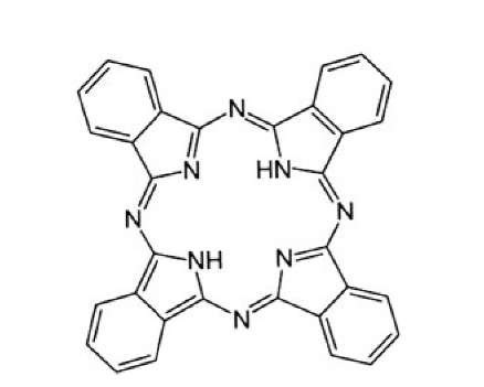
Figure 13.50. Example of a conjugated organic molecule (phthalocyanine) used for organic photovoltaic devices.
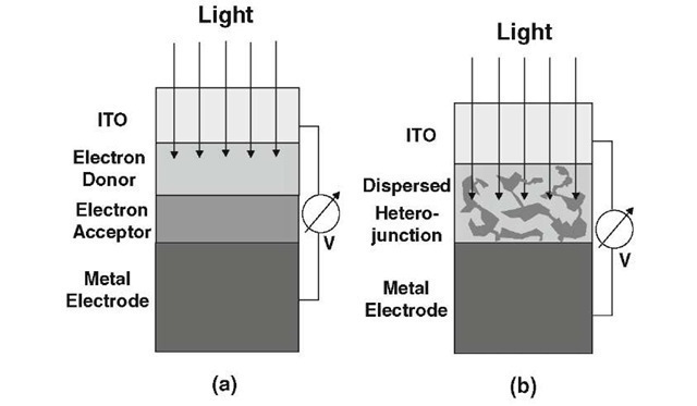
Further, due to the relatively weak field, electrons and holes do not separate fast enough from each other and recom-bine before they reach the electrodes. A double layer (heterojunction) organic photovoltaic cell provides some improvement; see Figure 13.51(a). The two layers in question consist of conjugated organics having different electron affinity8 and ionization energies. In short, the electrostatic forces generated at the interface between two properly selected organics of different electron affinity are significantly stronger compared to a single layer OPVC so that a more efficient dissociation (breakup) of the excitons is achieved.
Figure 13.51. Schematic representations of (a) a multilayer organic photovoltaic cell; (b) a dispersed heterojunction OPVC.
The layer which has the lower electron affinity is called the electron donor whereas the area with the higher electron affinity is termed to be the electron acceptor. (It should be noted that the terms donors and acceptors are not identical with the dopants in Si technology).
The performance of OPVCs can be further improved by dispersed (bulk) heterojunction solar cells. This enhancement is necessitated by knowing that polymer layers need to be at least 100 nm thick in order to obtain efficient absorption of light. However, the maximal diffusion length of exci-tons to the interface between organic layers may be only about 3-10 nm before the individual carriers recombine and thus seize to contribute to the solar energy collection. Thus, small electron donor domains and small acceptor domains (several nm in size) are mixed together to ensure short diffusion distances so that the excitons dissociate efficiently at the interfaces of these domains before they recombine; see Fig. 13.51(b).
Finally, similar to OLEDs, the efficiency of organic solar cells can be increased by stacking several OPVCs and connecting them in series to optimize the absorption of the incident light.
As in OLEDs, advantages of organic solar cells are their low production cost (utilizing spin coating or vapor deposition), mechanical flexibility, light weight, and high optical absorption coefficients. Interestingly enough, near infrared organic solar cells have been reported. However, disadvantages as of this writing are low efficiencies (up to 8% power conversion, that is, about 1/3 of the efficiency of silicon-based solar cells), low stability, and low strength. (The efficiency, that is, the light absorption can be improved by stamping optical fibers onto a polymer substrate that forms the foundation of the cell which acts as light pipes.) Moreover, during spin coating some solvents can degrade already existing layers. A further matter of concern is the mobility of the charge carriers. Specifically, some of the carriers may not reach the electrodes when their mobility is too low. Instead, they will recombine at trap sites or stay in the device and oppose the drift of new carriers, particularly if electron and hole mobilities are grossly different.
Liquid Crystal Displays (LCDs)
Many consumer products need to communicate the processed information to their owners, such as in wrist watches, calculator read-outs, video cameras, video recorders (VCRs), automobile dashboards, etc. Traditional cathode ray tubes (CRTs) as known for TVs and many computer monitors are still widely used. However, flat-panel displays are rapidly gaining ground. Among them, the liquid crystal display dominates with 85% this market, having annual sales near 15 billion dollars world-wide. LCDs had a 75% market share of the 200 million TVs produced in 2010. LCDs are "non-emissive devices", that is, they do not emit light by themselves, but rather depend on external illumination, as we will see momentarily.
LCDs contain peculiar viscous liquids whose rod-shaped molecules are arranged in a specifically ordered pattern. Each of these rod-shaped molecules has a strong electric dipole moment and can thus be oriented in an electric field, see Section 9.5. The viscous liquid is encapsulated in a glass container and is initially treated so that the molecules on one end are aligned at right angles to the ones on the other end; see Fig. 13.52(a). Moreover, the orientations of the molecules vary gradually from, say, a vertical to a horizontal array, as also depicted in Fig. 13.52(a). It is therefore called a "twisted nematic" type LCD.
If light which is polarized parallel to the aligned molecules of one end impinges on such a crystal, its electric vector will follow the twist of the molecules through the liquid crystal to the other end and emerges therefore on the opposite side with its polarization direction perpendicular to its original orientation. Since the analyzer that is placed behind the liquid crystal is oriented perpendicular to the polarizer, the emerging light beam is transmitted.
Figure 13.52. Schematic representation of a liquid crystal display unit (a) in the light-transmitting mode, (b) in the non-light-transmitting mode, caused by a potential that is applied to the end faces of the (twisted nematic) liquid crystal. Polarizer and analyzer are identical devices that allow the light (i.e., the electric field vector) to oscillate in only one direction as indicated by arrows (see also Section 13.1.2). The end faces of the liquid crystal-containing glass vessel are coated by transparent electrodes such as indium-tin-oxide (ITO).
On the other hand, if a small voltage (about 1 volt) is applied to the conducting end faces of the liquid crystal, the molecules (dipoles) align parallel to the field direction and the light is therefore not caused to change its polarization direction, see Fig. 13.52 (b). Thus, since polarizer and analyzer are mutually perpendicular to each other, the light is blocked from transmission. (If the polarity of the voltage on the crystal is reversed, the response of the LCD is not changed!)
In practice, a mirror is placed behind the liquid crystal arrangement which reflects the ambient light back to the viewer if the LCD is in the transmission mode. Alternatively, the display can be illuminated from the back to allow dark readability.
The advantage of LCDs is that they are inexpensive and that they consume very little energy (at least as long as no back-lighting is utilized). Moreover, they are compact, lightweight, portable, energy efficient, and pose lesser problems when recycling, compared to CRTs. On the negative side, LCDs cannot be read in the dark or in dim light without back-lighting. Furthermore, they have a limited usable temperature range (20°C to 47°C), slow time response, and most of all, they have a very narrow viewing angle. LCDs are matrix addressed by applying voltages to rows and columns, similarly as depicted in Fig. 8.45.
Emissive Flat-Panel Displays
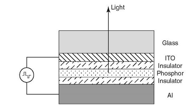
Electroluminescent devices utilize a thin phosphor film, such as manganese-doped zinc sulfide (ZnS:Mn), which is sandwiched between two insulating films, e.g., Al2O3 or Al-Ti-O (ATO). These films are surrounded by two conducting films (one of them being transparent indium-tin-oxide (ITO) on glass and the other a good reflector), see Fig. 13.53. The light emission is generally induced by an alternating (pulsed) electrical potential9 (about 120-200 V) applied between the two conducting electrodes. This generates an electric field amounting to about 106 V/cm across the phosphor layer, which causes an injection of electrons into the phosphor. Once the threshold voltage has been exceeded, the electrons become ballistic and excite the electrons of the activator atom in the phosphor (e.g., Mn) into a higher energy state. Upon reverting back into the ground state, photons of the respective wavelength are generated. As an example, a broad orange-yellow spectrum is emitted from the above-mentioned ZnS:Mn.
Figure 13.53. Schematic diagram of an electroluminescent device operated by alternating current pulses of about 200 V. The thin-film layers are about 300 nm thick except in the case of the phosphor, whose thickness is between 600 and 1,000 nm. The phosphor consists of the host matrix, such as a wide-band gap metal sulfide (ZnS, CuS, SrS), and an "activator", also called "luminescence center", such as Mn, Tb, Eu, Ce, Sm, Cu, Ag, etc.
The cost of electroluminescent devices is higher than for LCDs, but the viewing angle is wider and the usable temperature range is larger. They are rugged and have long lifetimes. Even though the luminescence efficiency is relatively good, readability in sunlight is still a problem. The response time is fast enough for video displays, but the power and voltage requirements (about 120-200 V) are difficult to obtain for small portable device applications. Electroluminescent devices comprise at present about 4% of the flat-panel market. They find applications in medical instruments, transportation, defense, and industrial equipment.
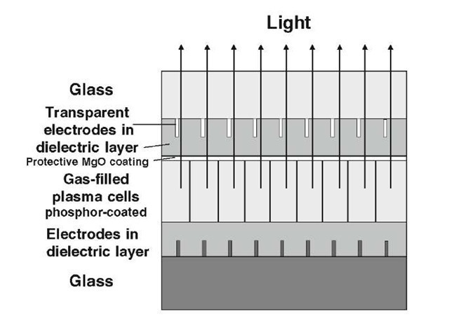
Plasma display panels (PDPs) operate quite similar to fluorescence light bulbs (Fig. 13.31). A relatively high AC voltage (100 V) is applied across a discharge gas (such as a helium/neon/xenon mixture) to create a plasma, see Figure 13.54. Recombination of electron-ion pairs in the plasma causes photons of high energy (that is, in the UV range). They are absorbed by phosphors which in turn emit visible light. Individually addressable compartments, which may contain different phosphors, yield the pixels needed for the three fundamental colors.
Flat-panel displays of this type are rugged, about 6 cm thick, provide deep blacks for better contrast ratios, the viewing angles are wide (up to 178°), and the lifetimes (at which there is a 50% reduction in light output) are estimated to be 100,000 hours. However, the pixel sizes are too large for small displays, that is, screens sizes below 32 inches diagonally are not on the market. On the other hand, large screen sizes up to 150 inches are quite popular. Because of high refresh rates and fast response times, there is essentially no blur for rapid motion which helps for displaying sports events etc.
Figure 13.54. Schematic representation of a plasma display (not drawn to scale).
PDPs are quite heavy because of two glass plates which hold the gases. The power consumption is high, for example, 400 watts for a 50 inch screen which is equivalent to cathode ray tubes. The colors tend to "wash out" in strong ambient light and the front glass causes a glare if no anti-glare layer is applied. Radio frequency interference by plasma displays may be disturbing to short wave and AM radio listeners. Plasma displays currently (2010) share about 8% of the TV flat-panel display market.
Field-emission displays (FEDs) are still in the experimental stage. They have much in common with cathode ray tubes (CRT), that is, with the bulky displays previously used for TVs and desk computers. Essentially, they consist of a matrix of tiny CRTs whereby each sub-CRT represents a single pixel. Electrons are "boiled-off" by thermionic emission (heat) from a large number of tip-shaped field-emitters (made of Mo, Si, Pt, or carbon nanotube cones), that can be matrix-addressed. They are encapsulated and hermetically sealed off in a thin cavity. A voltage between a grid, situated above the emitters accelerates the electrons to the front plate and there, causes to light a phosphor, covering the inside face of this plate by cathodoluminescence (see Section 13.8.1). FEDs require a vacuum which is at present, difficult to sustain for a long time. The aim is to build flat (about 1 cm thick) FEDs, having wide viewing angles and fast response times. It is anticipated that FEDs combine the high contrast level, and fast response time of CRTs with small power consumption in the range of 10-15 W.
The SED (surface-conduction electron-emitter display) is a variation of the FED and uses one emitter for each column instead of individual emitters.
Most of the flat panel displays are of the volatile type, that is, the pixels are periodically refreshed to retain their image. The refresh rate is typically several times per second which may cause eye irritation. For the non-volatile or static displays, the image requires energy to change. This mode is more energy efficient.
It is estimated that TVs account for 10% of a home’s energy use. For example, a 42-inch Hitachi plasma display draws 313 W of power (2007 value), whereas a same sized Sharp liquid crystal display is rated as 232 W (2009). It is feared that the energy use will rise as consumers will buy bigger, more elaborate TVs and watch them longer. The California Energy Commission recently mandated therefore a reduction of TV power consumption to <116 W by 2013.
Integrated Optoelectronics
Integrated optoelectronics deals with a family of optical components, such as lasers, photodiodes, optical waveguides, optical modulators, optical storage devices, etc., which are integrated on a common substrate (if feasible) with the aim of fulfilling similar functions as electrical integrated circuits do. The main difference to electrical devices is that in optical integrated circuits (OICs) the signal is transmitted by light. Still, they need in most cases electrical energy to become functional, which explains the name optoelectronic. Among the advantages of optical devices are reduced weight, the capability of light of different wavelengths to travel independently and simultaneously in the same waveguide (multiplexing), the immunity against receiving extraneous signals from surrounding devices by stray electromagnetic coupling (crosstalk), the difficulty in performing wire taps (because of the lack of electromagnetic fields, which would extend beyond the optical fiber), high reliability, speeds greater than electrons in a metallic wire, larger bandwidth (1012 Hz compared to 105 Hz for telephones) and notably, the low-loss transmission (<2 dB/km) of signals in optical fibers. Most of all, however, telecommunication utilizing laser optics, allows the simultaneous transmission of billions of telephone calls in one glass fiber, that is, as many simultaneous telephone calls as there are humans on earth! The sales of optoelectronic devices are presently in the neighborhood of 20-30 billion dollars worldwide!
We have discussed in previous topics two major optoelectronic components, the laser (Section 13.8) and the photo detector (Sections 8.7.6 and 8.7.7). A few more building blocks need to be added to complete the picture. This will be done now.
Passive Waveguides
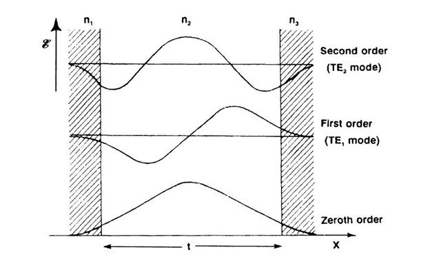
The interconnecting medium between various optical devices is called a waveguide. It generally consists of a thin, transparent layer whose index of refraction, n2, is larger than the refractive indices of the two surrounding media, n1 and n3. If this condition is fulfilled and if the light impinges on the boundary between n2 and n1 (or n3) at an angle which is larger than the angle of total reflection.10 then the optical beam travels in zigzag paths between the internal boundaries of Region 2. In other words, by undergoing total reflection, the light wave is considered to remain in the center region. This statement needs, however, some refinement. As a rule, the light which travels in the center medium extends, to a certain degree, into the neighboring media. The spatial distribution of the optical energy within all three media is called a mode. This spatial distribution can be calculated by solving the wave equation (10.4) while taking the appropriate boundary conditions into consideration. We have done this twice in earlier parts of this topic (Section 10.3 and Section 4.3). We learned there that the electric field strength or, equivalently, the intensity of a wave, decreases in the adjacent medium obeying an exponential function. If two boundaries need to be considered, as in the present case, and if the thickness, t, of the center region is comparable to the wavelength of light, then the solution of the wave equation yields an electric field strength distribution (as depicted in Fig. 13.55, lower curve). Now, we know from previous calculations (Section 4) that under certain conditions additional solutions, i.e., distribution functions, do exist (similarly, as a vibrating string can oscillate at higher harmonics). In the present case they are called first-order, second-order, etc., modes.
Figure 13.55. Electric field strength distribution (modes) in a waveguide assuming n1 — n3 (symmetric behavior). The zeroth order and higher-order modes are shown.
They are likewise depicted in Fig. 13.55. The reader probably recognizes that this "optical tunnel effect" is equivalent to the quantum mechanical tunnel effect shown in Fig. 4.8.
We now consider the most common case, in which n1 is considerably smaller than n3, e.g., n1 = 1 for air and n3 = 3.6 for GaAs (whereas n2 is still made larger than n3!). For this asymmetric case the condition for containing the light in the waveguide is
where 10 is the wavelength of the light in vacuum, k = 0, 1, 2 … is the mode number, and t is the thickness of the center layer. A calculation (see Problem 1) shows that the difference between n2 and n3 needs to be only about 1% in order to contain the light in the center medium.
Electro-Optical Waveguides (EOW)
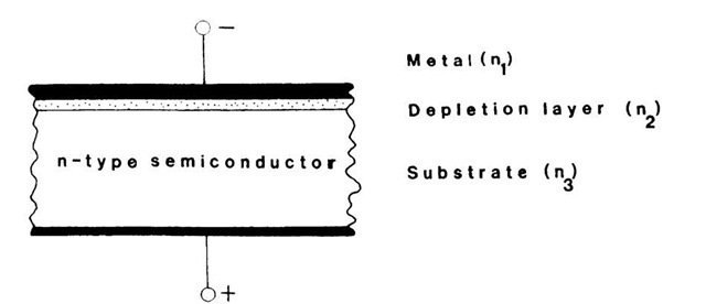
So far we tacitly implied that the various layers of a waveguide structure have been permanently manufactured by some type of deposition process out of the gaseous or liquid phase on a semiconducting substrate. This is indeed quite often done by employing, for example, molecular beam epitaxy or liquid phase epitaxy processes. However, a rather ingenious alternative method can be utilized instead. This technique involves a Schottky-barrier contact which, when reverse biased, forms (as we know from Section 8.7.2) a wide depletion layer (Fig. 13.56). We shall show in a short calculation that a depletion of charge carriers increases the index of refraction of a solid.
Figure 13.56. Electro-optical waveguide making use of a reverse-biased Schottky-barrier contact. (See also Fig. 8.15.) The light travels in Medium 2 (the depletion layer) when a high-enough voltage is applied to the device.
Recall that n2 > n3 (and n1) is the prerequisite for a waveguide structure. We derived in topic 11a relationship between the free carrier density (Nf) and the index of refraction,
where m* is the effective mass of the electrons in the medium, v is the frequency of light, e is the charge of the electrons, and n — n — ik is the complex index of refraction. We rewrite (11.7) twice for the substrate (Medium 3) and for the depletion layer from which some free carriers have been removed by the applied electric field (Medium 2).
The difference in the indices of refraction is then
which reduces with11
In the present case (transparent media) we can assume that the damping constant, k, in n — n — ik is negligibly small, so that n in (13.24) becomes a real quantity:
Equation (13.25) demonstrates, as suggested above, that a reduction in the number of free carriers from Nf3 to Nf2 causes an increase in the index of refraction in Medium 2. Then, the device becomes an optical waveguide. For this to happen, the doping of the substrate needs to be reasonably high in order that an appreciable change in the index of refraction is achieved (see Problem 4).

![tmp8-303_thumb[2][2][2][2][2][2] tmp8-303_thumb[2][2][2][2][2][2]](http://what-when-how.com/wp-content/uploads/2011/07/tmp8303_thumb222222_thumb.jpg)
![tmp8-305_thumb[2][2][2][2][2][2] tmp8-305_thumb[2][2][2][2][2][2]](http://what-when-how.com/wp-content/uploads/2011/07/tmp8305_thumb222222_thumb.jpg)
![tmp8-306_thumb[2][2][2][2][2][2] tmp8-306_thumb[2][2][2][2][2][2]](http://what-when-how.com/wp-content/uploads/2011/07/tmp8306_thumb222222_thumb.jpg)
![tmp8-307_thumb[2][2][2][2][2][2] tmp8-307_thumb[2][2][2][2][2][2]](http://what-when-how.com/wp-content/uploads/2011/07/tmp8307_thumb222222_thumb.jpg)
![tmp8-310_thumb[2][2][2][2][2][2] tmp8-310_thumb[2][2][2][2][2][2]](http://what-when-how.com/wp-content/uploads/2011/07/tmp8310_thumb222222_thumb.jpg)
![tmp8-311_thumb[2][2][2][2][2][2] tmp8-311_thumb[2][2][2][2][2][2]](http://what-when-how.com/wp-content/uploads/2011/07/tmp8311_thumb222222_thumb.jpg)
