Introduction
While the history of analog display interfaces can be viewed as starting with television and then moving into the computer field, digital display interfaces took the opposite course. This is not surprising; while computing systems may have first been developed in the analog domain, the digital computer very quickly came to be the only serious contender. The age of digital television, however, did not truly begin until technologies and hardware developed for computing began to be adapted for TV use.
Digital interfaces might seem to be a natural for the computer industry, and in fact (as was shown in the previous topic) the first display interfaces were of a very simple “digital” type. But the CRT display is not especially well-suited to a digital interfaces, and realizes few if any benefits from such.Discounting the general-purpose interfaces used with the early terminal-based systems, and the first crude CRT connections, the first widely successful digital display interfaces were those used with non-CRT types, in applications not readily supported by the CRT. The most obvious example of these are the displays used in calculators, “notebook” or “laptop” computers, and other such portable devices. These were for the most part, limited to embedded displays – those applications in which the display device itself is an integral component of the product, rather than being a physical separate peripheral. So the review of digital interface standards for displays begins with component-level interfaces. Later, however, as these alternative display technologies began to challenge the CRT on its traditional turf – desktop displays, such as computer monitors, and even larger non-portable devices such as television receivers – even the mainstream display interfaces have been forced to “go digital”.
Panel Interface Standards
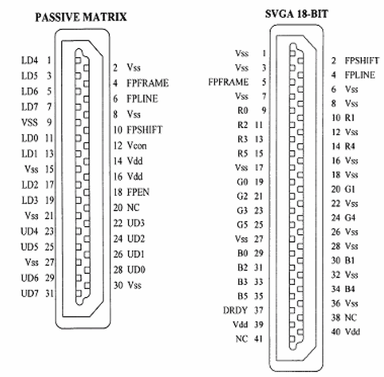
Early interfaces to LCD panels, as well of those for other technologies, were by no means standardized. To a large extent, this is true even today, although several industry standards have been developed, along with some de facto standardization around a particularly popular design or product line. Such interfaces were simply designed along with the panel and its integral driver ICs, to support the particular needs or capabilities of that design. There are, however, some features that these basic digital interfaces have in common. Almost always, the video data is organized by color, with only as many bits of input provided as are directly supported by the panel. In addition, the interface will typically provide a clock input, and the equivalent of the “horizontal and vertical sync” signals of the CRT interface – signals which, under whatever name, signify the start of a new line or new frame of data. The equivalent of a “blanking” signal, usually labelled “data valid”, “display enable”, or similar, is also provided, so that the loading of data into the panel can be inhibited without shutting down the input clock. It is also important to note that such interfaces do not always load the data into the panel in what might be the expected manner – one pixel per clock, scanning through the image in the conventional directions. Owing to the requirements of the various panel technologies, and to the desire for lower input data rates, simple digital panel interfaces often accept more than one pixel’s worth of data per clock (requiring more data connections). It is also common, particularly in “passive-matrix” LCD ,for the panel to be divided into two or more areas which will be loaded simultaneously (i.e., pixels will be loaded alternately into each area, scanning through these in the normal fashion, rather than proceeding strictly from left to right and top to bottom through the entire images. One of the earliest attempts to bring some standardization to this part of the industry – the first Flat Panel Display Interface standards (FPDI-I), introduced by the Video Electronics Standards Association (VESA) in 1992 – is shown in Figure 10-1. Note that in addition to the basic data and control interface, the physical connectors also typically provide lines intended for connection to external controls, such as “contrast” or “brightness” adjustments using off-panel potentiometers. Panel power is also typically provided via the same connector, although backlight power (generally requiring a much higher voltage, provided via a separate inverter) is often assigned a separate connection.
Figure 10-1 The VESA Flat Panel Display Interface (FPDI) standard connectors. This represents one of the earliest attempts to standardize the digital interface to LCD panels. Used by permission of VESA.
L VDS/EIA-644
One of the most successful attempts to bring order at the panel interface level began with the introduction of the Low Voltage Differential Signalling technology by National Semiconductor Corp. in the early 1990s. Commonly referred to as simply “LVDS,” it was also adopted by other manufacturers (notably Texas Instruments, which was the first second source of the product line), and was adopted as a standard by the Electronic Industries Association (later the Electronic Industries Alliance) as EIA-644.
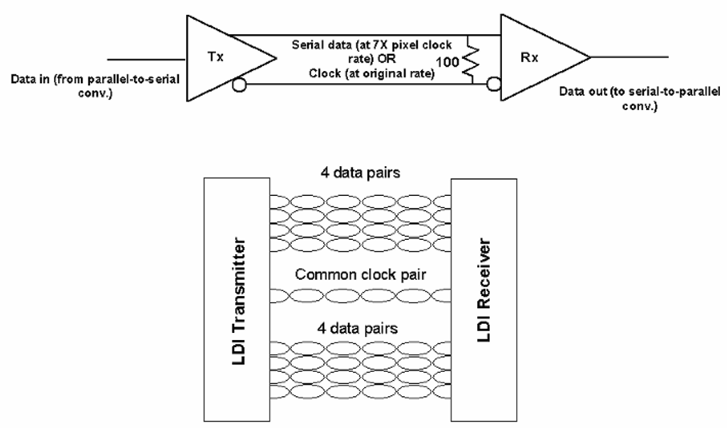
While viewed by many as only a display interface, LVDS is actually best viewed as a general-purpose, unidirectional digital data connection. In its most popular form for panel use, an LVDS transmitter IC is used to encode up to 24 bits of data per input clock onto four differential serial pairs. A slightly different version, commonly referred to as “OpenLDI” (for “LVDS Display Interface), was later introduced for monitor use, and basically just adds four additional data pairs for increased capacity (Figure 10-2). In either case, LVDS involves serialization of the input data, distributing it among the four (or eight) serial pairs, and transmitting it at a clock rate seven times the original. The pixel clock is also transmitted via a separate differential pair. All pairs, both data and clock, operate in a true voltage-differential mode, with a swing of 355 mV on each line; the system impedance is a nominal 100 Ω. The additional four bits per clock (4 data pairs times 7 bits/clock provides 28 bits on each clock pulse) are used to add four general-purpose control bits to the data transmission;in display applications, these are typically used to convey the line and frame sync signals, the display enable, plus one “custom” control signal to be used as required for a given application. An LVDS receiver accepts the data and clock pairs, uses the clock to both deserialize the data and to regenerate the original-rate pixel clock, and provides the video data, control signals, and clock as separated outputs.
Figure 10-2 The Low-Voltage Differential Signalling (LVDS) system. LVDS in its basic form essentially serializes and distributes incoming data among four differential pairs, along with a clock signal transmitted on a similar pair. The “OpenLDI” version of this interface (bottom) adds four additional data pairs (which share the original clock pair) for additional data capacity.
When first introduced, the LVDS system (also referred to as “Flat-Link™” by National Semiconductor, and “FPD-Link™” by Texas Instruments) was capable of operating with pixel clocks up to 40 MHz. This was soon extended to 65 MHz, then 85 MHz, and ultimately to 112 MHz, which is the current upper limit of any LVDS devices. In the basic 24-bit version, a 65 MHz connection will support a 1024 x 768 panel at a 60 Hz refresh rate (assuming a “CRT-like” timing, with lengthy blanking periods; if blanking can be reduced, up to an 80 Hz rate could be supported at this format). It is also, of course, possible to employ different data mappings with this link (such as 12 bits per pixel, 2 pixels per clock) which can potentially increase the supported frame rate. However, a more popular means of adding capacity to the LVDS system is simply to add additional data pairs. So-called “dual channel” LVDS inputs have become popular for large-format LCD panels, in which eight data pairs (normally used to convey two 24-bit pixels) are provided using a single, common clock pair.
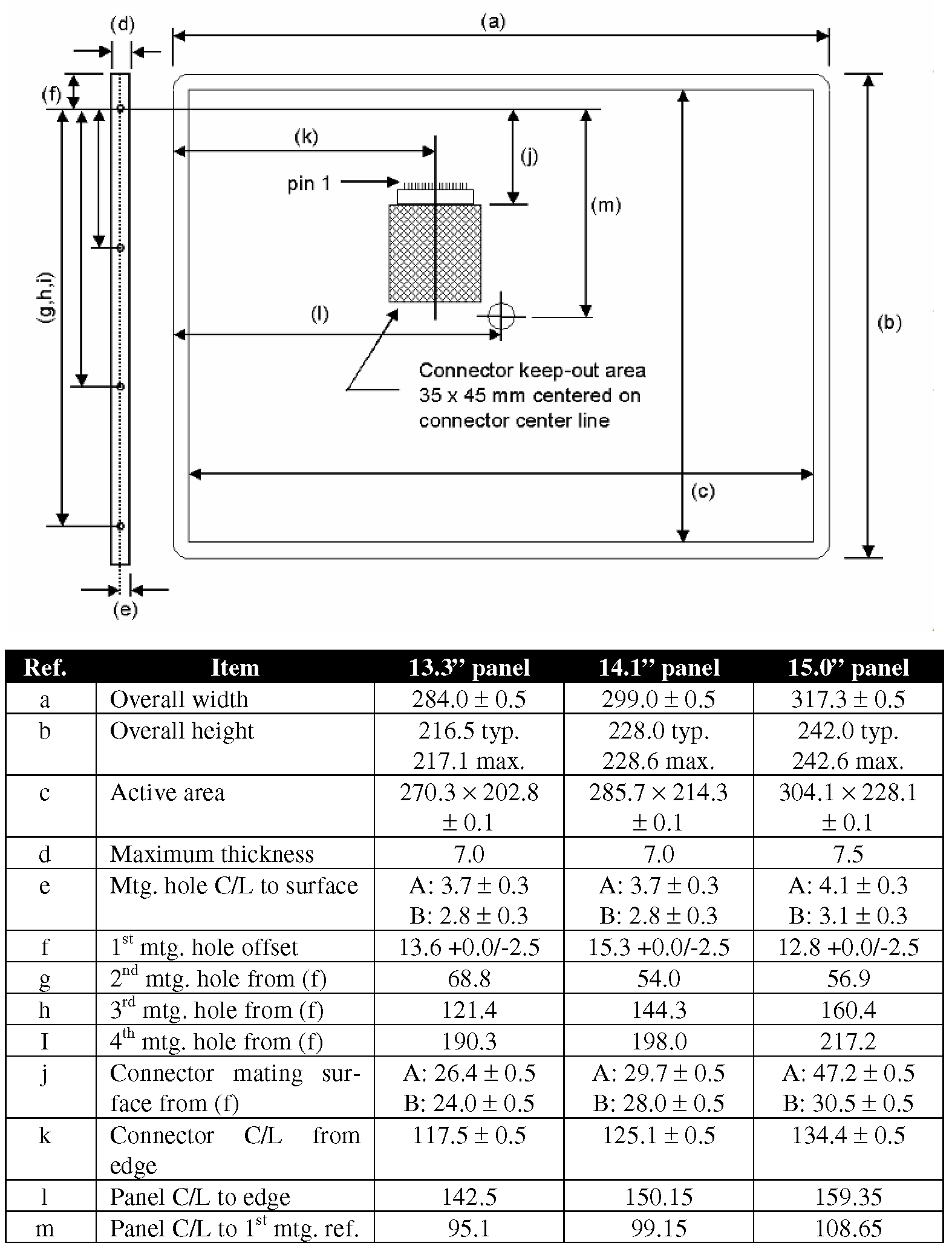
LVDS provides a relatively simple, efficient, and easy-to-use electrical interface, which has become extremely popular for flat-panel displays intended for embedded or integrated applications such as notebook computers. As such, it was also used as the basis for what has become the most popular industry standard for that market, the specifications published by the Standard Panels Working Group (SPWG). Formed in 1999 by seven notebook computer and display manufacturers (Compaq Computer Corp., Fujitsu, Hewlett-Packard Co., Hitachi, IBM Corp., NEC, and Toshiba), the SPWG’s intent was to standardize not only the electrical interface and physical connector, but also the panel dimensions and mounting hardware. Conformance to the SPWG specifications permit notebook computer manufacturers to use multiple sources for a given display. (However, the SPWG does not set standards for display performance, colorimetry, etc., so some care must still be exercised to ensure that displays from different sources are truly interchangeable.) The first SPWG specification set standards for medium-sized, medium-format notebook displays: 10.4 inch, 12.1 inch, and 13.3 inch diagonal panels, of the “SVGA” and “XGA” (800 x 600 and 1024 x 768, respectively) formats, using a single (4 data pairs) LVDS channel. The SPWG 2.0 specification, released in 2000, provides similar standards for larger panels (up to 15.0 inch diagonal, and up to the “UXGA”, or 1600 x 1200, format) using a dual-channel (8 data pairs) interface. A summary of the SPWG specifications is given in Figures 10-3 and 10-4; the complete specifications are available directly from the Standard Panels Working Group (www.displaysearch.com/SWPG).
Figure 10-3 Summary of SPWG 2.0 mechanical specifications. All dimensions in mm. Tolerances ± 0.3 mm unless otherwise indicated. Note: The SPWG 2.0 specification established two different panel types, referred to as “A” and “B”, with differences as noted above. The “B” style, which is proposed for all designs from 2003 on, is intended to encourage a move toward thinner panels.
Figure 10.4 SPWG pinouts (per SPWG 2.0). The 2.0 version of the SPWG specification defines two connectors, as shown here. The 20-pin connector is for Style A XGA panels only; the 30-pin connector is used for SXGA+ (and above) panels of either style, and all Style B panels.


