The True Advantage of Digital
From the preceding discussion, the reader may now be under the impression that there is no real advantage to digital interfaces over analog, or that the author is somehow “anti-digital”.
This is not the case; the purpose so far has been to show that the terms “analog” and “digital” do not, as is commonly assumed, describe two vastly different and unrelated fields of study, and in fact are governed by the same basic constraints as any other electrical system. Many of the supposed differences between the two do not have anything to do with how the information to be transmitted is encoded, but rather on completely unrelated factors.
Given this, why should we expect a continued transition away from the established analog standards and toward the much-hyped “all-digital” future? It should now be apparent that, as long as “digital” interfaces are being used in a manner that simply duplicates the functions of their analog predecessors, there is little practical impetus for such a change.
However, the advantage of digital interfaces, for display applications as well as many others, lies not in the advantages at the interface itself but rather what providing information in this form will enable. The true advantage of digital encoding of video information lies in the ease with which such information may be processed and stored. In the analog domain, storing even a single frame – let alone a significant portion of a video stream – requires complex and relatively expensive equipment, and the quality of the signal will inevitably be degraded by the process. And there are also no practical analog means through which the image information can be significantly altered: you cannot change the image format, the frame rate, etc., readily. But all of these and more are easily achieved in the digital domain through inexpensive processors. Digital memory sufficient to store hours of video has become relatively cheap – and this storage will be essentially “perfect”, with no degradation of the image quality at all. Digital signal processing and storage is also the primary enabling factor in practically all of the recent advances in display systems – from the compression techniques used to make HDTV a practical reality, to the encryption techniques used to protect copyrighted imagery, and on to the scaling and processing methods that make fixed-format displays a viable alternative to the traditional CRT. These are what truly makes a digital representation worthwhile, and each is covered in some depth in later topics.
Performance Measurement of Digital and Analog Interfaces
Before proceeding on to review current analog and digital interface standards, it is appropriate to look at some of the techniques and terminology used to measure and describe signal quality in each type. In both cases, observation of the signal itself, at relevant points in the system, via an oscilloscope (and often more sophisticated equipment) remains the primary means of determining signal “goodness.” However, there are different areas of concern for analog and digital signalling, and somewhat different terminology used to describe the relevant points of each. There are also some additional, more specialized techniques which should be covered, having to do with the characterization of other parts of the system.
Analog signal parameters and measurement
Many of the parameters and measurements discussed in this section have been defined, at least for computer video purposes, by the VESA Video Signal Standard (VSIS) and the related VESA test procedure document, “Evaluation of Analog Display Graphics Subsystems.” Similar standards and procedures have been published by such bodies as the EIA and SMPTE. The reader is directed to those standards for further information on the specifics for each.
A typical analog signal, as might be seen on an appropriate wideband oscilloscope, is shown in Figure 6-5. This might be one small portion of an analog video transmission, but in showing several transitions it demonstrates many of the important parameters for video signal characterization. In this example, the signal in question includes synchronization pulses (as is common in television practice, but rarely seen in computer display systems), but the concepts will apply to any analog video system.
First, assuming that we have ensured that the source of this signal is delivering a full “black to white” swing, observation of the signal provides a quick check of the absolute and relative amplitudes of the signal and its various components. Note that most analog video systems are intended for use with AC-coupled inputs at the display or receiver, and so a measurement of the signal offset from the local reference (ground) may or may not be meaningful. Besides the amplitudes themselves, though, the signal behavior during the transitions is among the most important observations that can be obtained from such a view. The parameters which describe this behavior include the following.
Figure 6-5 A portion of a typical analog video signal as it might appear on an oscilloscope, showing a horizontal sync pulse and a transition from the blanking level to the reference white level. Rise and fall times for such signals are normally measured between the 10% and 90% points on each transition, as shown. Note the “ringing” (damped oscillation) which follows each transition.
Rise/fall time
Among the most basic of indicators of the “sharpness” of the video signal – and related to the bandwidth of the channel required for its successful transmission – are the rise and fall times. These are as indicated by item “a” in Figure 6-5, and are simply measurements of the duration of the transition, between specified points. Typically, standard rise and fall time measurements are made between the 10% and 90% of full-scale points, on a full-amplitude (i.e., from “black” to “white”) transition. It is possible, of course, to use other defined points – and one might ask why the 0% and 100% values are not used instead. The reason for this is the difficulty of locating these points at a time which is unambiguously part of the transition itself, and not during some other transient event such as the overshoot/ringing portions of the transition.
Overshoot/undershoot; settling time
As in any practical system, the signals observed in analog video interfaces will never show “perfect,” instantaneous transitions between any two states. Owing to the ever-present reactive elements in any real circuit, there will always be some degree of “overshoot” and “ringing” associated with a change of signal level. These are typically as shown in Figure 6-6. While they are unavoidable, careful attention to the design and construction of the interface, and especially the termination components, can greatly minimize their impact. If small enough in both amplitude and duration, these phenomena will have essentially no visible effect on the displayed image. (“Undershoot” is commonly used to refer to the same phenomena as “overshoot”, but on a negative-going transition. We will assume that the two can be treated identically here.)
Figure 6-6 Overshoot, ringing, and settling time. The ringing following the full-range transition of Figure 6-5 is magnified here, showing details of how overshoot and settling time are defined.
The amplitude of the overshoot may be given simply by noting the amount to which the final steady-state amplitude of the signal is exceeded. In other words, referring again to Figure 6-6, the overshoot amplitude is Vmax – Vss (or in the case of undershoot, Vss – Vmin). However, unless the over/undershoot is truly excessive, an even more important concern may be the settling time. This may be characterized by noting the time between a given point of the transition – commonly, either the 90%-of-full-scale point, or the first point after the initial overshoot when the signal passed the final, steady-state value, are used – to the time at which the signal settles to within a certain margin (typically, ±5-10%) of the final value.
Other parameters of potential concern are not readily observable from a simple observation such as this, and require either specific signals or reference to other signals for their determination. These include jitter, skew, integral and differential linearity, and monotonicity. Signals representative of those used to measure these factors are shown in Figures 6-7 and 6-8. Note that jitter and skew are measures of the signal’s accuracy and stability in time, relative to a given reference. In typical analog video systems, this reference may be a sampling clock (if one is provided or accessible), or more commonly the synchronization signals used by the system. Skew, jitter, and other mismatches (including those of amplitude) may also be characterized between multiple analog channels, as in an RGB three-channel video interface.
Skew
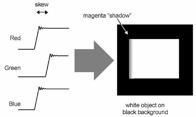
Skew is the difference in temporal location of supposedly simultaneous events between two (or more) channels. For example, Figure 6-7 shows a situation in which the three channels of a video interface are all supposed to be making identical transitions (this might represent the start of a white area on the display), but the green is noticeably later than the other two. The time difference, as measured between identical points on the waveform, would then be stated as the skew between the two signals (or between a given signal and an agreed-to reference). In terms of the appearance of the resulting image, this particular case would result in what should have been a clean black-to-white transition on the screen appearing to have a magenta “shadow” to the left (Figure 6-7b). Skew results from mismatches in the path delay of one channel relative to another, either from physical length differences in the channel (cabling, PC traces, etc.) or different cumulative propagation delays within discrete components.
Figure 6-7 Skew. Here, the green signal transition has been delayed relative to the red and blue; this might result in the appearance shown at right, as what was supposed to have been a white square has a magenta edge. Should the transition back to the black level be similarly delayed, there would also of course be a green edge on the right side of the square.
Jitter
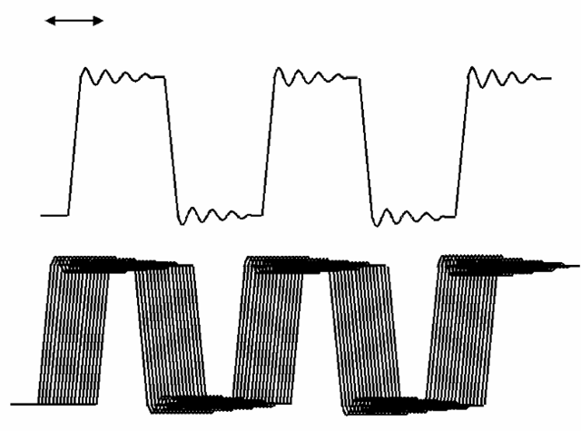
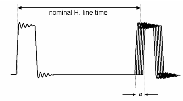
Jitter is similar to skew, in that is relates to the location of a particular portion of the waveform in time, but differs in that skew refers to a steady-state error while jitter is the amplitude of expected or observed transient temporal errors. Jitter may, in other words, be viewed as the “noise” in the location of the waveform in time, relative to another signal or established reference. Most often, jitter is observed by using the system clock (the clock intended for sampling or latching the signal in question) as the trigger or reference for the oscilloscope observing the signal, and noting the amplitude of the variation in the signal edge position. This is shown in the example of Figure 6-8.
Jitter may also occur, and be measured, between a given reference point within a signal and a later point within that same signal; in this case, it represents the cumulative timing in-stability or error between the two points. An example of this is shown in Figure 6-9, in which a horizontal sync pulse edge has been defined as the reference point, and the jitter is being measured as the maximum peak-to-peak variation in the location of the subsequent edge.
Figure 6-8 Jitter. Here, the upper trace is used as the reference clock, and we are observing the jitter (temporal instability relative to the reference) of a similar signal shown below. The excursion in time of the edge of the signal being measured, relative to the reference, is the jitter; it may be expressed in terms of the absolute maximum jitter, average, etc..
Figure 6-9 Jitter within a single signal. In this case, the position of the leading edge of a horizontal sync pulse is observed to be unstable relative to the preceding pulse; i.e., the duration of a horizontal time is not perfectly fixed.
Linearity
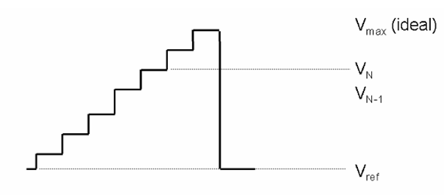
Linearity error can refer to either non-linearities introduced into a signal as it has been passed by a supposedly linear operation (i.e., an amplifier) or in the generation of that signal (as in the digital-to-analog converter (DAC) common to most computer-graphics video outputs). Linearity may be specified and measured in a number of different ways. The VESA video standard defines two measurements for linearity, differential and integral. This assumes, as is often the case in computer graphics systems, that the analog signal is being created under the control of digital signals (via a digital-to-analog converter), and so may be expected to have discrete and identifiable “steps” from one value to the next. With reference to Figure 6-10, differential linearity is stated as the difference between adjacent values, normalized to the expected value corresponding to one LSB change (and therefore is ideally 1.000). Expressed mathematically, this is
The integral linearity error, on the other hand, is simply the difference between the actual signal level at any given point, compared to its ideal value, again normalized to the ideal LSB value, or
Figure 6-10 Linearity. In this simple example, the output of a 3-bit (eight level) digital-to-analog converter is being checked. There are obvious linearity problems, as not all transitions are of equal amplitude. The differential linearity error is the difference between the amplitude of a given transition and the theoretical value for that transition; in this case, a transition of one least-significant-bit (LSB) should be equal to the ideal![]() (Note that the LSB value for an N-bit system is
(Note that the LSB value for an N-bit system is![tmp7ee190_thumb[2] tmp7ee190_thumb[2]](http://what-when-how.com/wp-content/uploads/2012/06/tmp7ee190_thumb2_thumb.png) The integral linearity error is the total error between the measured amplitude at a given level, and the theoretical value for that level (for level N, this is
The integral linearity error is the total error between the measured amplitude at a given level, and the theoretical value for that level (for level N, this is![tmp7ee191_thumb[2] tmp7ee191_thumb[2]](http://what-when-how.com/wp-content/uploads/2012/06/tmp7ee191_thumb2_thumb.png)
As noted, these direct measurements of signal linearity are based on the assumption that the signal is, in fact, created as a series of discrete steps. It is also possible to measure and express linearity error by arbitrarily selecting reference points on the input signal, and then noting the error between the actual and expected value (assuming a linear process) of the output signal.
Historically, other measurements have been used to indirectly measure the linearity of a given analog system. These generally are based on the fact that non-linearities in a system will result in the generation of spurious spectral components, not present in the original signal but related to the original components. An example of one such is the statement of the total harmonic distortion (THD) of a system, which is a measurement of the energy present in such spurious harmonics as a percentage of the total output signal.
Transmission-line effects and measurements
As noted above, analog signals are susceptible to distortion and error arising from improper terminations and similar “transmission-line” concerns. While the effect these have on the signal can certainly be characterized through many of the measurements already discussed, it is important to be able to recognize such situations when they are seen.
The only real difference between what are classed as “transmission-line” phenomena and other non-ideal behaviors of a system is the introduction of a time factor; the delay introduced by the physical length of the transmission channel. This has the effect of separating, or spreading out in time, the effects of distortion-causing elements. For example, the most common “transmission-line” problems generally result from impedance mismatches at various point in the signal path, and the reflections which result from these. In simple circuit analysis, an incorrect impedance results only in less efficient power transfer. But if a significant time delay is introduced between a signal source and the load, or receiver, of that signal, the analysis becomes significantly more complex. The lumped impedance of the source, the distributed or characteristic impedance of the signal path (the physical conductors), and the termination of that path provided by the receiver, plus the path length between all points of concern, must all be considered.
Consider Figure 6-11 a, which shows a simplified version of an idealized analog video system. Analog video specifications have generally been written assuming a system impedance standard of 75 Ω, as is shown here. And should all of the indicated impedances exactly meet this requirement, no problems arise. However, in Figure 6- 11b, an impedance mismatch exists; in this case, the characteristic impedance of the video cable is incorrect. This results in reflections being generated at the cable endpoints, as shown, and the resulting distortion of the signal. In video systems, depending on the length of the path between signal source and receiver (and so the delay between the two) such reflections can result in the visible effect known as “ghosting” of images in the display. However, the distortion of the signal “edges” or transitions will often result in more subtle effects. Deviations from the ideal here, as in Figure 6-12, can result in changes in the system timing should they occur on an edge used as a clock or timing reference, such as would be the case with a synchronization signal or sampling clock edge. Sufficient distortion may even result in additional, spurious triggering of the circuit the signal is to clock.
Detection and characterization of such problems in practical systems can be done through observation of these effects in the signal as viewed at the source or receiver, but more specialized equipment is also available to analyze transmission-line systems. The time-domain reflectometer, or TDR, is a common example. This device operates by launching pulses into the signal path, and analyzing the magnitude, polarity, and timing of the reflections it then sees. Such instruments are capable of providing considerably more detailed looks at the system’s impedance characteristics, including detection of mismatches.
Figure 6-11 Transmission-line effects in video cabling. In a properly matched system (top), source, load, and cable impedances are all identical (the standard for video is a 75-Ω system impedance, as shown here), and the video signal may be transmitted with no reflections at any point. If any of the impedances do not match, as in the lower figure, the impedance discontinuity at that point generates a reflection. In this example, a cable of the incorrect impedance has been used, making for a mismatch condition at both the source and load end. Inserting a 50-Ω cable into a 75-Ω system results in a reflection coefficient![]() of 0.2 at both; any pulse arriving at either termination will produce a reflection of 20% the amplitude of that pulse. With reflections produced at both ends of the cable, such conditions can result in visible “ghost” images, in addition to causing the signal integrity problems discussed in the text.
of 0.2 at both; any pulse arriving at either termination will produce a reflection of 20% the amplitude of that pulse. With reflections produced at both ends of the cable, such conditions can result in visible “ghost” images, in addition to causing the signal integrity problems discussed in the text.
Figure 6-12 Impedance mismatches may also result in problems at signal transitions, as shown here. In this example, a mismatch results in an initial transition to a lower amplitude than would otherwise be the case; the next transition to the final value does not occur until the reflection has returned from the other end of the cable. Should the first transition – and possible subsequent ringing – occur around the switching threshold of an input connected to this line, in the case of a logic signal, such distortions of the signal edge can result in unwanted triggering.
Digital systems
From the earlier discussion, it should be apparent that “digital” and “analog” signals are not really different in kind; the two classifications are, after all, simply different means of encoding information onto what remains just an electrical signal. Therefore, it should not be surprising that many of the same problems can impact “digital” systems, and many of the same measurements are still relevant. Obviously, some will not be; in a simple binary-encoded system, for instance, the linearity of the channel conveying the signal is not of particular concern. However, rise and fall time, jitter, skew, and so forth are still very much a concern in many digital applications. Even greater importance is often assigned to those factors that may affect the “edges” or transitions of the signal, due to the often-greater importance of the timing of these transitions in digital systems.
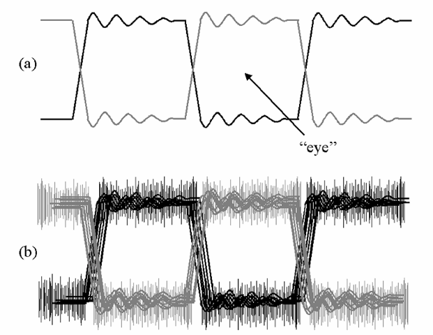
Due to the nature of most digital systems, however, a single, relatively simple examination of the signal can often serve to determine the acceptability of the system’s performance. In the majority of digital systems, the primary concerns with the signal’s integrity center on being able to unambiguously identify one of two possible states at certain discrete points in time, as determined by a clock signal. Therefore, if the signal can be determined to provide sufficient noise margin, and to be settled at the correct level at the time of the active clock edge, the system may be expected to perform correctly. This may be quickly checked through the observation of the “eye pattern” using an oscilloscope. An eye pattern is produced by generating a signal with approximately a 50% average duty cycle (i.e., it spends as much time in the high state as in the low); alternating between the two states is ideal. Using the appropriate clock signal as the trigger source (the same clock which the intended receiver would normally use to sample the data), the oscilloscope timebase is adjusted such that multiple states of the signal are displayed within the same portion of the screen. This results in the pattern shown in Figure 6-13a.
Figure 6-13 Eye patterns. Commonly used as a quick visual check of digital signal quality, an “eye pattern” is produced by causing transitions of the signal in question to overlay on an oscilloscope display as shown in (a). Noise on the signal, amplitude deviations, jitter, etc., will all tend to close the “eye,” as shown in (b). The open area of the eye shows the period during which the states of the signal can be properly distinguished in both amplitude and time; should the “eye” close entirely, the signal is unusable.
Most digital oscilloscopes, and many analog instruments with storage or “variable persistence” features, may be set to show multiple samples of the signal, overwritten upon each other. Unless each has exactly the same amplitude and timing characteristics, differences here will show up as a “smearing” of the signal traces around the nominal amplitude values and edge locations (Figure 6-13b). The effects of jitter smear the location of the signal edges in time; noise and amplitude errors smear the trace in the vertical axis. The worse either or both of these become, the more “closed” the “eye” (the inner portion of each period) will appear. Should the eye close entirely, or at least to the point at which the state of the signal cannot be unambiguously determined during the expected sampling time, the transmission will experience errors.


![tmp7ee186_thumb[2] tmp7ee186_thumb[2]](http://what-when-how.com/wp-content/uploads/2012/06/tmp7ee186_thumb2_thumb.png)
![tmp7ee187_thumb[2] tmp7ee187_thumb[2]](http://what-when-how.com/wp-content/uploads/2012/06/tmp7ee187_thumb2_thumb.png)
