Amplifier
Amplification is the process that increases the signal magnitude. Thus, an amplifier is a component that does just that. Unlike most filters, an amplifier is an active component and requires power to accomplish its function. Note that the ideal amplifier would only increase the amplitude of the signal. However, any commercial amplifier will not only increase the amplitude but also add noise to the resulting signal. The goal, of course, is to have a component that amplifies the signal and adds minimal noise.
The fundamental parameters used to describe an amplifier are
1. gain, usually expressed in dB, and often assumed constant over a
2. specified frequency range; and a
3. noise figure, again usually expressed in dB, and indicative of the amount of noise that will be added to the signal being amplified.
Note that this discussion simplifies the practical amplifier. We are assuming the amplifier is a packaged device, ignoring the actual fabrication. Further, parameters such as the third-order intercept point, power requirements, and maximum power handling are all additional factors that could be considered but are neglected to simplify the discussion.
Also the amplification shown in Figure 4.2 shows a single amplifier capable of 50 dB gain. It would be unusual to have a single amplifier capable of such gain. What is represented as a single amplifier in Figure 4.2 can be constructed of cascaded multistage amplifiers.
The goal of the amplifier is to raise the extremely weak incident signal to a level practical for analog-to-digital conversion. Thus, the amount of amplification is based on the specific ADC and will be discussed in that section. Further, there is typically a distribution of amplification or gain across different frequencies for reasons that will become obvious in the next subsection.
Mixer/Local Oscillator
The basic function of the mixer/local oscillator combination is to translate the input 1575.42 MHz RF carrier to a lower intermediate frequency (IF) and preserve the modulated signal structure. The most obvious reason for this is to bring the frequency to usable ranges in which to operate on the signal, in particular perform the analog-to-digital conversion. However, there are fewer obvious reasons for the frequency translation, as is discussed within this subsection.
The design illustrated in Figure 4.2 utilizes a single stage of analog frequency translation. However, it is possible to utilize multiple stages of analog frequency translation in a single front-end design. The choice is a design trade-off based on the components available and their individual specifications. The focus of this section is to illustrate the functionality of the single-stage approach shown in Figure 4.2.
First, it is important to discuss the individual components. The local oscillator for GNSS front-end designs is typically a combination of components. Most crystal oscillators, either standalone or temperature compensated/ovenized for greater stability, are not capable of generating the desired local oscillator frequency for the L1 GNSS signal. Thus, a phase lock loop (PLL) is combined with the crystal to achieve the desired higher frequency of the local oscillator. In addition, it is common practice that the local oscillator be divided down to serve as the sampling clock, as shown in Figure 4.2. This is an important aspect as a single frequency source, and any associated frequency error/drift, will serve as the basis for the receiver.
The mixer operates through the trigonometric identity expressed as
It is possible to use the front-end design in Figure 4.2 as an example of the mixing process. In this case &>i equals the GNSS L1 center frequency 1575.42MHz and the desired IF is 47.74 MHz, then the desired local oscillator frequency m2 would be (1575.42 – 47.74) MHz = 1527.68MHz. Any modulation, such as the GNSS spreading codes and navigation data, can be simply expressed as a time-varying multiplier:
In this case it is obvious that the output of the mixer will be the sum and difference frequencies. Of interest here is the difference frequency, which is at the desired IF. The sum frequency is simply a consequence in this case, and the second filter depicted in the cascade of Figure 4.2, which follows the mixer, is used to select only the desired difference frequency.
Note that in Figure 4.2 a bandpass filter is used for this process. However, given the fact that the goal is to simply remove the sum component, a lowpass filter should be more than sufficient. In many cases this is true; however, Equations (4.3) and (4.4) present a simplified model of a mixer, which in reality is more complicated. Mixer parameters include conversion loss, isolation, dynamic range, and intermodulation. In this case the bandpass filter is selected to minimize any complications from intermodulation products that result from the mixing. For this simplified discussion, only the straightforward model of the mixer is presented.
With the combination local oscillator/mixer it is now possible to translate the RF carrier to a lower IF. It has been eluded to above that this is required for the analog-to-digital conversion process, but is that the only reason? Are there other reasons as to why frequency translation is important in GNSS receivers? The answer is "yes" with two immediate additional justifications for the frequency translation.
The first is the quality and cost of the component. The goal of this text is to develop software GNSS receivers for the narrowband L1 signals, with the definition of narrowband being 2-8 MHz (see Problem 7). It is important to recognize that it can be quite difficult to fabricate narrowband filters at high frequency.
Denote the quality factor of the filter by Q, the center frequency of the filter (1575.42MHz for GNSS L1) by![]() and the bandwidth of that filter by BW.
and the bandwidth of that filter by BW.
Then the quality of a filter is defined by
If we assume a 3 dB bandwidth and desire a filter to capture the main lobe of the GPS spectrum (2.046 MHz wide), the Q factor for such a filter comes out to be 770—an extremely high value. To put things in perspective, fabrication of most commercial filters (although it does depend on the technology) sets a minimal bandwidth of 2% of the center frequency. This corresponds to a Q value of 50, significantly less than the 770 computed above.
However, perform the same computation at the resulting 47.74 MHz IF from the design in Figure4.2. That Q factor is 47.74/2.046 or 23.33, which is a much more realizable filter. Thus, the frequency translation to IF allows higher frequency selectivity with less costly/complex components.
The second additional factor motivating frequency translation is feedback. The amount of amplification in the RF chain is tremendous; over 100 dB of gain is applied. If this is all attempted at a single frequency, then it is highly likely that feedback will become an issue unless meticulous shielding and spatial separation across the RF chain is implemented. Otherwise, if the 100+ dB of gain were applied all within the 1575.42 MHz band even with quality RF cabling between components, it is unlikely to prevent feedback within the amplification stages in the RF chain. Utilizing multiple stages within a front-end design allows the gain to be distributed across frequency. For example, in the single-stage downconver-sion depicted in Figure 4.2 the gain within the RF chain is split between the RF and IF paths. Thus the level of shielding and potential for feedback are reduced as the output of the lower-frequency amplifiers cannot feedback into the input of the higher-frequency amplifiers.
Analog-to-Digital Converter
The final component in the front-end path is the analog-to-digital converter. This device is responsible for the conversion of the analog signal to digital samples. There is a wide variety of ADCs available on the market, with a dizzying set of parameters for each. Consider, for example, the Texas Instruments ADS830 ADC, see focus.ti.com/lit/ds/symlink/ads830.pdf. Such an ADC has an overwhelming number of parameters, the majority of which are not discussed here. An application note can help users sort out the various parameters associated with ADCs; see Anonymous (2000).
The key parameters to consider for this discussion are the number of bits, the maximum sampling frequency, the analog input bandwidth, and the analog input range.
The CDMA nature of the GNSS signal requires very little dynamic range from the sampled signal. It has been shown that if single bit sampling is used, then degradation in the resulting processing is less than 2 dB; see Bastide et al. (2003). Further, if conservative 2- or more bit sampling is utilized with proper quantization, the degradation is less than 1 dB. The minimum number of bits on most commercial ADCs is 8 as is the case for the ADS830. Thus, in designing a GNSS front end, it is most convenient to either utilize a hard limiter to obtain a single bit or use a commercial ADC taking all or just a subset of the resulting bits of each sample. It is also important to recognize that if multibit sampling is employed, then some form of gain control must be implemented to provide proper quantization.
One might ask if the penalty for using single bit sampling is less than 2 dB, why any front end would utilize multibit sampling and then incorporate the overhead associated with automatic gain control? The key point to remember is that the less-than 2 dB penalty is for the ideal case. If, for example, there exists narrowband interference within the GNSS L1, then single bit sampling will be captured by the interference source and prevent GNSS processing. Thus, although the theoretical penalty for single-bit sampling is less than 2 dB, the nature of the operating environment may dictate the need for multibit sampling.
The maximum sampling frequency is an interesting parameter. This frequency needs to accommodate the bandwidth of the desired signal. Continuing to use the ADS830 part as an example, the maximum sampling frequency is 60 MHz and thus can provide a resulting sampling bandwidth of 30 MHz, more than sufficient for the narrowband L1 navigation signals. However, recognize that the IF in Figure 4.2 is at 47.74 MHz, which is greater than the resulting [0-30] MHz sampled information bandwidth. In this case, the sampling process acts as a second frequency translation stage.
Although the ADC has a sampling frequency that provides an upper limit of 30 MHz on the resulting sampling bandwidth, then analog input bandwidth of this ADC really determines what signals will be captured. For the ADS830, this value is an impressive 300 MHz. What this means is that any frequency component input to the ADC up to 300 MHz will be aliased according the sampling theorem.
Should the analog input bandwidth have been as high as 1.6 GHz, which is not impossible (see pdfserv.maxim-ic.com/en/ds/MAX104.pdf), then it would be possible to directly sample and alias the original RF signal. Such an implementation has been demonstrated yet there remain many technical hurdles to overcome with such an approach. The approach outlined does provide the means to compute an appropriate sampling frequency and the resulting sampling IF.
Based on the preceding discussion, the role of the final filter in the RF chain becomes clear. It must be a bandpass filter and limit the band to only those frequencies to be preserved through the sampling process. Recognize that the aliasing does not only occur for the desired IF, but all frequencies within the analog input bandwidth of the ADC. Thus, it is critical for minimal noise that the last filter prior to the ADC allows only those frequencies of interest and attenuates all others within the analog input bandwidth.
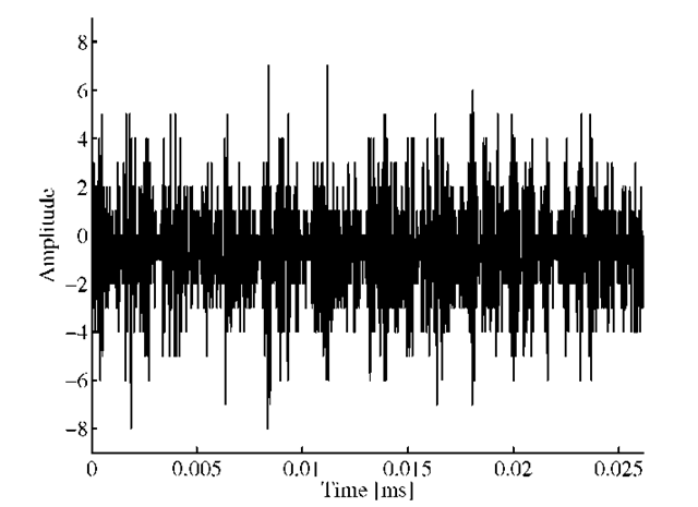
FIGURE 4.4. Time domain. Representation of 1000 samples.
Referring to the design in Figure 4.2, a sampling frequency of 38.192MHz is used for the 47.74 MHz IF, and this provides a final digital frequency translation to an IF of 9.548 MHz. The resulting sampled information bandwidth of [0-38.192/2] MHz provides more.
The final ADC parameter to be discussed is the analog input range. This range defines the voltage range for which the quantization will be distributed across. In the case of the ADS830 part, the minimum analog input range is 1 V peak-to-peak. Assuming a 50 ^ load, which is traditional in radio frequency design, a 1 V signal corresponds to — 17dBW. Thus, it should now be clear why the amplification within the RF chain is needed. It had been mentioned that it was to provide suitable signal levels. The combination of thermal noise and received signal will be simply too weak to exercise the bits in this or any ADC. So a goal of the amplifiers is to increase the received signal level, which again is dominated by the thermal noise, to exercise the full range of the ADC.
Although not depicted in Figure 4.2, the final amplifier in many GNSS front-end designs will be a variable gain with a feedback signal resulting from processing implemented after the ADC. This is implemented and known within most GNSS receivers as automatic gain control (AGC). The goal of the front end is to exercise all available bits with the ADC. Thus, if the gain is insufficient to do so and this is determined by monitoring the sampled data stream, the gain can be increased. Alternatively, if the gain is too high such that the outer ADC bins have an overwhelming number of samples, then the gain can be decreased. Lastly, as will be discussed when the sampled data are presented, the AGC can be steered by the expected distribution of the sample bins. In this way, the front end can attempt to minimize the impact of narrowband interference.
In summary, the object of the bulk of the components within the front end is to condition the voltage incident on the antenna for sampling by the ADC. In order to accomplish this for most ADCs there are three basis functions which must be accomplished.
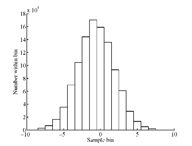
FIGURE 4.5. Histogram of 1,048,576 data samples.
These are amplification, frequency translation/downconversion, and filtering. These prepare the signal for analog-to-digital conversion, which results in the samples to be processed within the software receiver.
Resulting Sampled Data
Now that the operation/functionality of the GNSS front end has been described, it is worthwhile to highlight the resulting data that have been collected from the front-end design depicted in Figure 4.2 and have been included on the media with the topic.
Again, the important parameters for the signal processing are
- Sampling frequency: 38.192MHz
- Intermediate frequency: 9.548 MHz, and
- Four-bit samples.
The above parameters provide all the necessary information for the operation of the signal processing algorithms. Some other items, such as the time and date and approximate location of the data collection, can speed the acquisition as will be discussed, but are not required.
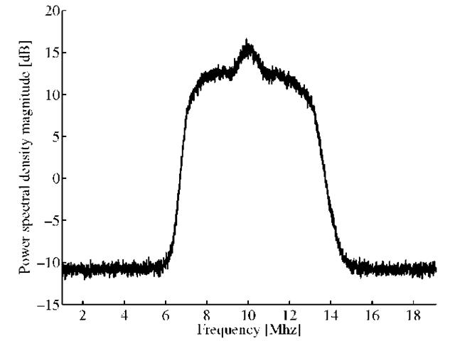
What can be done is to show the resulting digital samples in typical representations. Thus, in Figures 4.4, 4.5, and 4.6, a time domain, histogram, and frequency domain depiction of the collected data are illustrated, respectively.
In the time domain depiction, no discernable structure is visible despite the 9.548 MHz IF for the collected GPS data. In the histogram, it is obvious that all four bits of the ADC are being triggered based on the 16 levels present within the histogram.
FIGURE 4.6. Frequency domain. Representation of 1,048,576 samples of GPS L1 data.
Also the histogram bears a strong resemblance to the probability density function for a Gaussian random variable, which would be expected for white thermal noise. These plots follow what would be expected based on the frequency domain depiction in Figure 4.1 where the thermal noise would dominate the resulting samples.
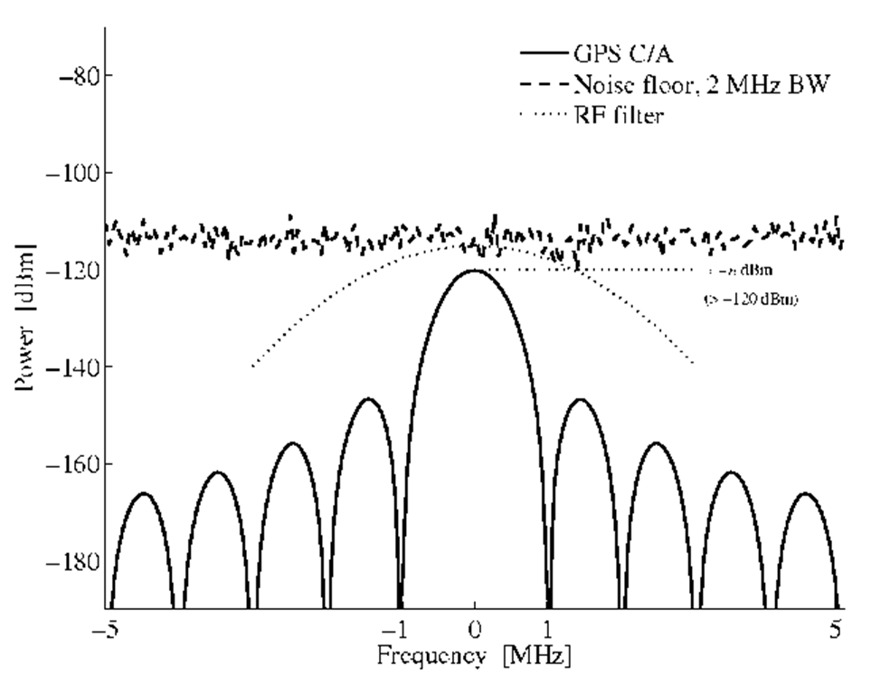
However, the frequency domain depiction does not resemble Figure 4.1; rather some obvious structure is present. This structure is best explained by building on Figure 4.1, as shown in Figure 4.7.
In this figure, obvious changes have been made to better correspond to the frequency domain depiction of the collected data file.
First, the "noise level" is not white, or flat and uniform as a function of frequency, but has some definite structure. This is a result of the final bandpass filter prior to sampling. This 6 MHz-wide bandpass filter shapes the spectrum of the analog signal to be sampled. Thus, the filter shape has been added within Figure 4.7.
Second, there is an obvious "bulge" within the center of the passband right at the resulting IF of the GPS translated signal. This actually appears to be the main 2.046MHz lobe of the sinc spectrum of the signal itself. With the specified received signal power level so much lower than the expected thermal noise, how can there be any discernable structure from the satellite signal from a data set collected with a traditional hemispherical antenna? The explanation has two components:
- the individual received satellite signal power is currently higher than the minimum specified (as shown in Figure 4.7); and
- the CDMA nature of the GPS system has all the satellite signal power overlaid at the resulting IF; thus, the spectrum shows the summation of all the visible satellite signal power.
FIGURE 4.7. Improved frequency domain depiction. Center frequency 1575.42 MHz.
These two factors bring about some, although minimal, structure from the satellite signal spectrum into the frequency domain representation of the collected data.
For the most part, the data indeed resemble thermal noise, and all the traditional GNSS signal processing is required to acquire, track, and utilize the navigation transmission.
GNSS Front-End ASIC
The final section of this topic presents the current state of the art for GNSS front-end designs. The implementation in Figure 4.2 has been built from expensive discrete components. Although this provides a high-quality front-end suitable for a lab instrument or environment, the cost for such an implementation can approach $5000. With the cost of handheld GPS receivers now well below $100, an alternative to such a design must exist.
The solution comes in the form of an integrated circuit. The bulk of the functionality of Figure 4.2 has been incorporated by multiple vendors into an ASIC that is typically smaller than 5 x 5 mm packages and utilizes less than 50 mW; see SiGe SE4110L, Nemerix NJ1006, and Texas Instruments TRF5101 data sheets. Such components strive to be as completely self-contained as possible, requiring only a minimal number of external components.
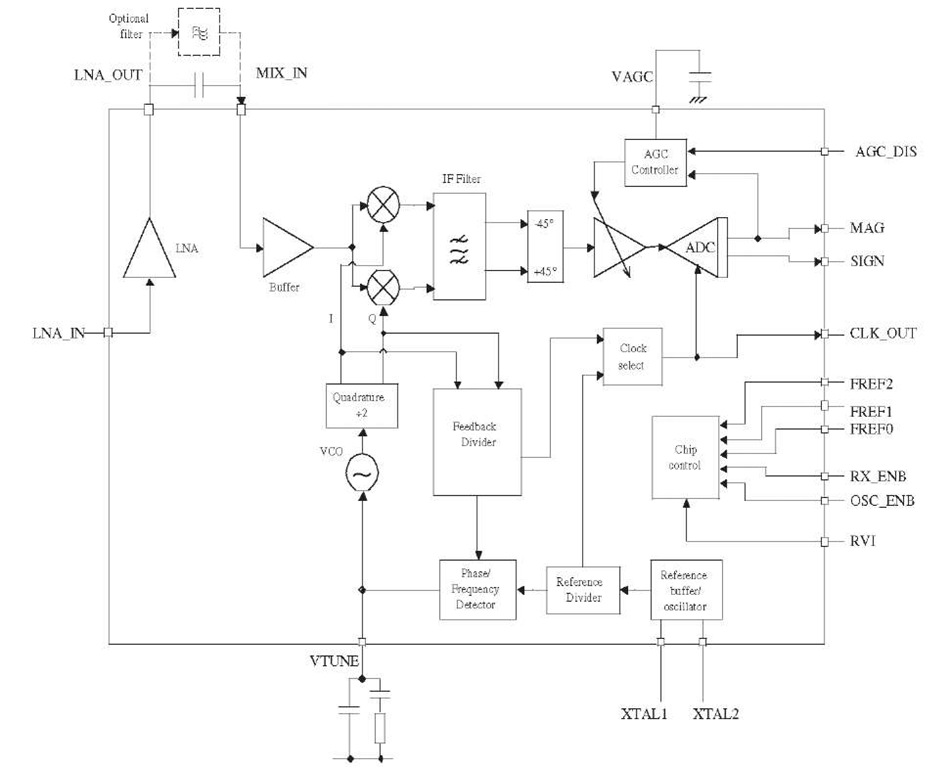
For example, consider the block diagram for the SiGe SE4110L component shown in Figure 4.8. This is an excellent example of a GPS front-end ASIC component. The complete data sheet for the SE4110L is included on the bundled DVD.
FIGURE 4.8. Block diagram of the SE4110L front-end ASIC.
Based on the discussion within the topic, the underlying design of the component should be somewhat familiar. A single-frequency translation stage is utilized along automatic gain control functionality to support multiple bit sampling.
It is quite impressive to see the level of integration within such a component. It utilizes a traditional antenna input (although a passive antenna can be used with an internal LNA with noise figure of less than 2.5 dB) and provides 2-bit digital samples supporting a number of different clock frequencies for a variety of applications. This particular part is only 4 x 4 mm and draws less than 10 mA from a nominal 2.7-3.3 V supply. Such integration is even more impressive when one considers the gain required for processing the received signal power of the GPS and potential feedback issues.
Such development even further facilitates the wide scale deployment of satellite navigation technology at a relatively low cost.
The ASIC-based front end is just one of multiple options for converting the signal in space to a digital format suitable for the software based signal processing. The goal of this topic is to provide some insight into the source of that data.
![tmp2D780_thumb[2] tmp2D780_thumb[2]](http://what-when-how.com/wp-content/uploads/2012/02/tmp2D780_thumb2_thumb.png)
