Motivation
The acquisition provides only rough estimates of the frequency and code phase parameters. The main purpose of tracking is to refine these values, keep track, and demodulate the navigation data from the specific satellite (and provide an estimate of the pseudorange). A basic demodulation scheme is shown in Figure 7.1.
The figure shows the scheme used to demodulate the input signal to obtain the navigation message. First, the input signal is multiplied with a carrier replica. This is done to wipe off the carrier wave from the signal. In the next step, the signal is multiplied with a code replica, and the output of this multiplication gives the navigation message. So the tracking module has to generate two replicas, one for the carrier and one for the code, to perfectly track and demodulate the signal of one satellite. In the following, a detailed description of the demodulation scheme is conducted.
Demodulation
Let![]() be the carrier frequencies of L1 and L2 for the signal transmitted from satellite k with powers
be the carrier frequencies of L1 and L2 for the signal transmitted from satellite k with powers![]() for C/A or P code. The C/A code sequence is
for C/A or P code. The C/A code sequence is![]() and the P(Y) code sequence is
and the P(Y) code sequence is![]() If the navigation data sequence is called
If the navigation data sequence is called![]() the total signal is given as
the total signal is given as
FIGURE 7.1. Basic demodulation scheme. This scheme is used to demodulate the navigation message.
The output from the front end including Altering and downconversion can be described as
where![]() is the intermediate frequency to which the front end has downconverted the carrier frequency. Equation (7.2) describes the output of the front end from one satellite.
is the intermediate frequency to which the front end has downconverted the carrier frequency. Equation (7.2) describes the output of the front end from one satellite.
This signal is then sampled by the A/D converter. Because of the narrow bandpass filter around the C/A code, the P code is distorted. In this way the last term in Equation (7.2) is filtered out and cannot be demodulated and is in the following described as noise![]() The signal from satellite k after the A/D conversion can be described as
The signal from satellite k after the A/D conversion can be described as
with n in units of![]() indicates that the signal is discrete in time.
indicates that the signal is discrete in time.
To obtain the navigation data![]() from the above signal, the signal has to be converted down to baseband. The carrier removal is done by multiplying the input signal with a replica of the carrier as shown in Figure 7.1. If the carrier replica is identical to the incoming carrier in both frequency and phase, the product of both is
from the above signal, the signal has to be converted down to baseband. The carrier removal is done by multiplying the input signal with a replica of the carrier as shown in Figure 7.1. If the carrier replica is identical to the incoming carrier in both frequency and phase, the product of both is
where the first term is the navigation message multiplied with the PRN code and the second term is a carrier with the double intermediate frequency. The latter part of the signal can be removed by applying a lowpass filter. The signal after the lowpass filter is
The next step is to remove the code![]() from the signal. This is done by correlating the signal with a local code replica. If the code replica is exactly the same as the code in the signal, the output of the correlation is
from the signal. This is done by correlating the signal with a local code replica. If the code replica is exactly the same as the code in the signal, the output of the correlation is
where![]() is the navigation message multiplied by the amount of points in the signal N.
is the navigation message multiplied by the amount of points in the signal N.
FIGURE 7.2. Linearized digital second-order PLL model.
The above description of the demodulation is only for a signal with one satellite. This is done to reduce the complexity of the equations and to give a simpler idea of the demodulation scheme. In the real signal there is a signal contribution from each visible satellite resulting in larger noise terms in the equations.
In the demodulation scheme seen in Figure 7.1, two local signal replicas are required. To produce the exact replica some kind of feedback is needed. The feedback loop to produce the carrier replica is referred to as the carrier tracking loop, and the feedback loop to produce the exact code replica is referred to as the code tracking loop.
Second-Order PLL
Both the carrier tracking (Costas loop) and code tracking [delay lock loop (DLL)] have an analytic linear phase lock loop model that can be used to predict performance.Another excellent reference, once the fundamental models for Costas and DLL have been derived, for linear phase lock loop and its parameters and performance is by Best (2003).
Extending the linear PLL model has been derived by Chung et al. (1993). This approach will be followed by the implementation of both the Costas loop and DLL, yet the linear model references earlier can still be the basis of performance prediction and analysis.
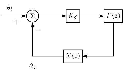
The second-order PLL system contains a first-order filter and a voltage controlled oscillator (VCO). Note that the transfer function of an analog loop filter and a VCO are
where F (s) and N (s) are the transfer functions of the filter and NCO, respectively. ![]() is the NCO gain. The transfer function of a linearized analog PLL is [refer to Chung etal. (1993)]
is the NCO gain. The transfer function of a linearized analog PLL is [refer to Chung etal. (1993)]
FIGURE 7.3. Second-order phase lock loop filter.
where![]() is the gain of the phase discriminator. Substituting Equations (7.7) and (7.8) into the transfer function (7.9) yields
is the gain of the phase discriminator. Substituting Equations (7.7) and (7.8) into the transfer function (7.9) yields
where the natural frequency![]() and the damping ratio
and the damping ratio![]()
![]() The above transfer functions are analog versions and to convert the transfer functions to digital form, the bilinear transformation is used on (7.10). This yields the following digital transfer functions for the PLL model:
The above transfer functions are analog versions and to convert the transfer functions to digital form, the bilinear transformation is used on (7.10). This yields the following digital transfer functions for the PLL model:
The linearized digital second-order PLL model is shown in Figure 7.2, where![]() is the discriminator gain, F (z) is the transfer function of the filter, and N(z) is the transfer function of NCO. The transfer functions for the digital filter and NCO are
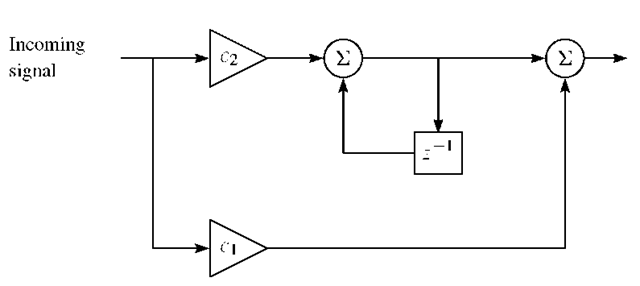
is the discriminator gain, F (z) is the transfer function of the filter, and N(z) is the transfer function of NCO. The transfer functions for the digital filter and NCO are
where F (z) is the transfer function of the filter and N(z) is the transfer function of the NCO. Figure 7.3 shows the phase lock filter F (z).
The goal is to find the coefficients![]() and
and![]() in the second-order PLL. This is done by comparing the transfer function for the digital PLL and the transfer function for the analog PLL. The transfer function for the digital version can be found as
in the second-order PLL. This is done by comparing the transfer function for the digital PLL and the transfer function for the analog PLL. The transfer function for the digital version can be found as
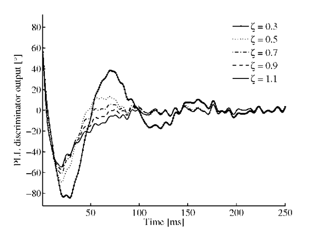
FIGURE 7.4. Phase error as function of different damping ratios![]() A larger settling time results in a smaller overshoot of the phase.
A larger settling time results in a smaller overshoot of the phase.
By substituting (7.12) and (7.13) into (7.14), we obtain the following:
To find an equation for the two coefficients![]() (7.11) and (7.15) are compared. This yields the following two equations:
(7.11) and (7.15) are compared. This yields the following two equations:
where![]() is the loop gain,
is the loop gain,![]() is the damping ratio,
is the damping ratio,![]() is the natural frequency, and T is the sampling time; see Chung et al. (1993). The natural frequency can be found as
is the natural frequency, and T is the sampling time; see Chung et al. (1993). The natural frequency can be found as
where![]() is the noise bandwidth in the loop.
is the noise bandwidth in the loop.
The damping ratio and noise bandwidth are computed for a particular signal case. But in some cases an engineer would like to change these values for specific applications or implementations. Therefore, a more thorough explanation is given about these parameters.
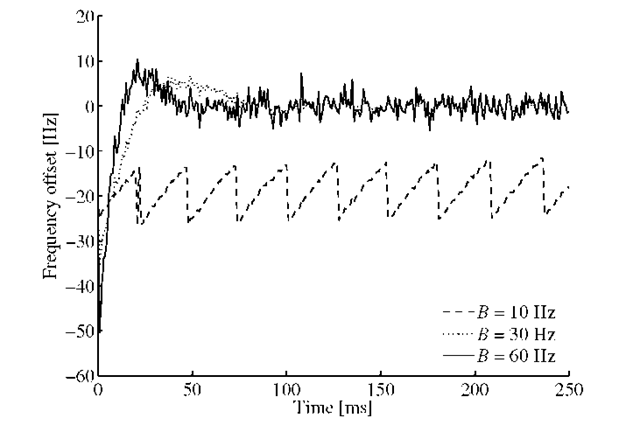
FIGURE 7.5. Frequency offsets from an acquired frequency offset 20 Hz and for PLL noise bandwidths of 10, 30, and 60 Hz. There are negative peaks in the first 2 ms due to transition phase in the loop filter.


