Chemistry Reference
In-Depth Information
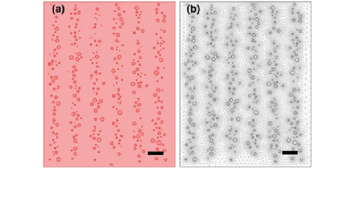
Fig. 2.8 A simulated geometry of a holographic sensor with a multilayer grating. a Organisation of
Ag
0
NP stacks within a hydrogel matrix, b Forming a geometric mesh of the Ag
0
NP pattern. Scale
bars = 150 nm. Reproduced from [
83
] with permission from The Royal Society of Chemistry
ne the radii of the Ag
0
NPs. The mean value of the radii was set to
4
-
24 nm with
˃
= 5 nm. After generating the Ag
0
NP patterns in MATLAB
®
, they
were imported into COMSOL Multiphysics
®
for modelling. The pattern of Ag
0
NP
was surrounded with a square domain of a medium that is analogous to a hydrogel
matrix. The remaining Ag
0
NP subdomains were set to have an electrical con-
ductivity of Ag
0
(61.6 mS/m). Since Ag
0
NPs absorbs electromagnetic radiation, a
complex refractive index was required. This absorption does not signi
used to de
cantly affect
the propagation of light when a small number of stacks are simulated. However, the
absorption can reduce the ef
ciency of diffracted light in a holographic sensor that
have a high number of Ag
0
NP stacks. Figure
2.8
b illustrates the geometric mesh of
the holographic sensor in COMSOL Multiphysics
®
. The incident electromagnetic
waves were propagated from left to right along the array of Ag
0
NP stacks. The left
boundary of the cell was set to a scattering boundary condition. The light source
was de
ned as a plane wave of varying wavelengths [
95
]:
n
r
H
z
ð
Þ
jkH
z
¼
jk 1
ð
k
n
Þ
H
oz
exp
ð
jkr
Þ
ð
2
6
Þ
:
where n is the complex refractive index, H
z
is the magnetic
field strength at position
r, k is the propagation constant, and H
oz
is the initial magnetic
field strength.
2 nm to resolve each Ag
0
NP. Once meshing was established, a computation was performed via a parametric
sweep, which allowed solving for a range of wavelengths. The wavelength
parameters set covered 400
Meshing was performed with a
finite element size of
*
900 nm. Finally, using
“
power out
fl
ow and time
-
average
boundary integration, the transmitted waves were collected at the opposite
side of the holographic sensor. Figure
2.9
a
”
-
c illustrates the simulated geometry that
resembles the con
guration of a typical holographic sensor, and Fig.
2.9
d shows the