Chemistry Reference
In-Depth Information
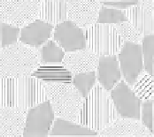
Fig. 4.1
Schematic representation of nanostructures as a function of their dimensionality
up a few tens of nanometres, typically less than 100 nm while nanocrystalline
alloys obtained by subsequent annealing of an amorphous precursor consist of
nanocrystalline grains embedded in an amorphous remainder. The case of nano-
structured powders refer to rather dense packing of nanograins or aggregation of
nanoparticles which can be obtained by different physical routes: an example is the
high energy ball milling.
Such a description of materials gives unambiguously evidence of the increasing
role of the surfaces, interfaces or grain boundaries when the size of the nano-
objects is decreasing, particularly below 20 nm as observed in Fig.
4.2
. In addi-
tion, it does affect some physical properties as the chemical reactivity, mechanical,
structural, electronic, vibrational, magnetic, and transport properties, by compar-
ing to those of bulk or massive analogous crystalline materials. The understanding
of changes of these physical properties requires a good knowledge of each of the
constituents, i.e. the chemical composition and the structure of the particles, grains
and layers on the one hand and those of the surfaces, grain boundaries and
interfaces on the other hand. The challenge consists thus in the characterization of
these different contributions in order to model both the global physical properties.
The main questions lye on the elaboration of such nanomaterials and their
reproducibility, their chemical and structural homogeneity at different scales, their
chemical stability with atmosphere, temperature, ageing, … and then the relevance
of their physical properties to make them good candidates for applications.
The investigation of physical properties of microcrystalline solid state materials
is usually performed by a complementary set of diffraction techniques, micros-
copies and different spectroscopic tools, in addition to calorimetric methods and
magnetic measurements. Indeed, the modelling of diffraction patterns allow to
establish the structural nature and to estimate the lattice parameters while trans-
mission electron microscopy (TEM) can bring an insight on the presence of
structural defects, providing the sample has been successfully thinned. In the case
of magnetic materials, it is concluded from the usual static magnetic measurements
combined to neutron diffraction to the establishment of magnetic structure and the
estimation of the magnetic characteristics.
In the case of nanomaterials, the diffraction patterns exhibit a broadening
of Bragg peaks: the modelling which requires special methodology included in
Rietveld refinement, gives rise to an estimate of the mean lattice parameters and
the mean coherent diffraction domain size and its mean morphology, i.e. shape and


